
How to Relate the Probe You’re Using to the Measurement You’re Taking
If someone were to ask you what one singular device is most synonymous with testing, or even electrical engineering, the overwhelming response would most likely be the oscilloscope probe (referred to as a probe). No other device has been through the hands of more students from measuring their first resistor divider to biasing their first MOSFET. Engineering students were taught that by connecting the probe to the circuit the oscilloscope will represent the signal as it appears in the circuit, without affecting the circuit. In a sense, without realizing it, many of us started out visualizing a probe connected to the circuit under test (CUT) as depicted in Figure 1.
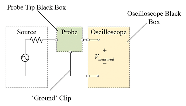
Figure 1: How engineers are introduced to probes
It is not until later in many engineer’s careers that the more nuanced portions of the probe come into play while testing memory circuits, and we move from understanding it as Figure 1, to understanding it as Figure 2.
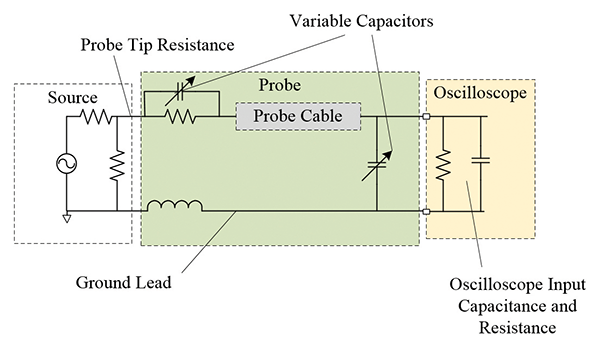
Figure 2: An expanded probe model
Understanding how we go between these figures, the effect it has on the measured signal, and how to account for those effects necessitates a need for an understanding of parasitics and circuit theory which starts at understanding the characteristics of probing and measurement in general. After establishing a basic understanding of what makes up a probe, using examples it will be shown how that probe can negatively affect the CUT it’s meant to measure as well as solutions to those problems. After this identification, remedies to these effects will be exploredby pointing explaining the different types of probing hardware available so you can make the most accurate measurement possible.
After finishing this article, it is my hope that you (the reader) will gain a thorough understanding of the various characteristics of what makes up a good measurement and how probes can make a bad measurement; and to be critical of your measurement system.
The Ideal Probe… Isn’t So Ideal
A variety of probe and probe attachments are available to the average engineer, but without knowing how the physical characteristics of the probe are altered by these attachments all that extra hardware may be left in the box while your scope signals suffer. We begin explaining these by establishing the physical circuit model of a non-ideal probe. Here it is important to pay attention to values found on the datasheet such as:
- Probe tip resistance;
- Probe tip capacitance; and
- While lead inductance is not stated, usually probes come with a variety of different ground clips to attach to your circuit depending upon the signal and application.
Before we start adding these characteristics together to create a basic probe model, we start with a basic circuit as shown in Figure 3, a probe connected to a voltage divider.
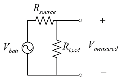
Figure 3: The basic voltage divider circuit
This is a basic DC model of a probe, where the probe tip resistance, or input resistance of the probe is shown to be in parallel with the CUT. This probe input resistance is usually very high as the oscilloscope needs some current to recreate the signal, but it only needs a little bit of current to do so; so, values range from the 1MΩ to 10s of MΩ. This input resistance scales with attenuation ratios as well, the DC model of a probe is shown in Figure 4.
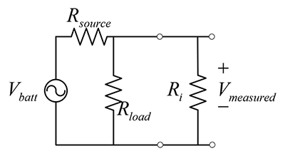
Figure 4: The voltage divider with probe resistance
Now, at AC is when the other two characteristics, the input capacitance and the different connectors are added. To examine these effects, we start with the figure previously described, instead we first add the probe tip capacitance or input capacitance. This value can range from 200pF for a normal probe to less than 5pF, for a low capacitance probe. I’m sure many offices have something called a “low cap(acitance) active probe,” for when you need to measure that pesky clock signal. With the addition of capacitance to our probe circuit model, we now get Figure 5.
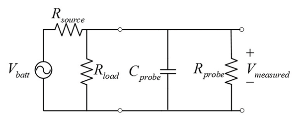
Figure 5: The voltage divider with probe capacitance
And usually the only way to control the capacitance of a probe is either through spending more or through compensation.
Lastly, we have the inductance associated with the ground clip which is the partial inductance associated with the measurement loop. This is something that probe manufacturers do not specify, but instead give ‘hardware’ to the customer in the form of different ground connectors to match the measurement with the application. The most typical connector found on most probes utilizes a long ground lead with an alligator clip on the end, which could result in an inductance in the measurement return path greater than 100nH at times. We can update our figure to form a complete model of a scope probe now to what is shown in Figure 6.
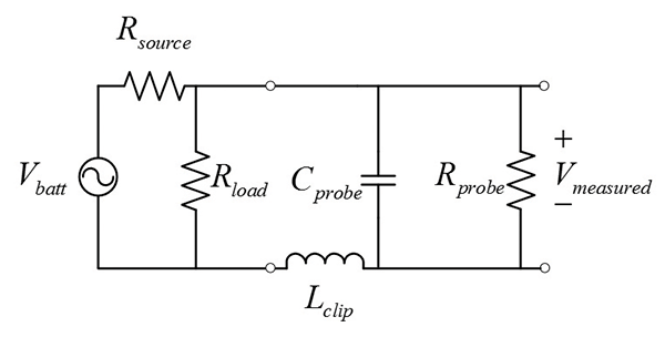
Figure 6: The complete probe model, with lead inductance
Now that we have a basic probe model, along with how the physical makeup of the probe effects these parameters one should already be asking- “When would we ever connect an inductor in the return path of a measurement signal?” The answer most give is that they would, of course, never do such a thing, but, of course, we do it all the time.
The next step is to investigate the effect these characteristics have on a circuit being tested.
How Do Probes Affect Your Measurement?
Now that a probe model has been established, we begin to see that the oscilloscope probe is not as ideal as first thought. Oscilloscope probes have effects on the load at both DC and AC that depend upon the three additional circuit components shown. An overview of how these circuit components effect the circuit being tested are:
- The measurement device can load the source at both DC and AC depending upon the input resistance, capacitance and the lead inductance. This results in effects on rise/fall time due to capacitance loading, ringing due to the lead inductance and overall dynamic measurement range of the system.
- Now that reactive components have been identified, there will be notable effects on the amplitude and phase of the measured signal.
- While the bandwidth of the oscilloscope is of main concern, that is usually controlled for and should far exceed the measurement bandwidth of the system resulting in the bandwidth of the probe being our biggest concern.
Using SPICE and our example circuit shown in Figure 7, we can examine some of these effects and how it causes inaccuracies in the measurement.
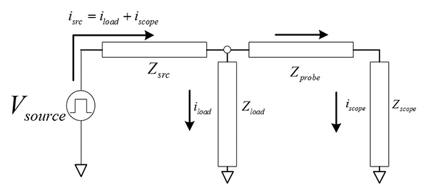
Figure 7: A signal source being measured, and the applicable impedances
DC Source Loading
This leads us to our first practical limitation of a probe when you connect it to a circuit you want to measure at DC, referred to as DC source loading. DC source loading deals with the finite amount of current that the probe and thus the oscilloscope needs to develop a signal voltage at the oscilloscope’s input. When connected to the CUT, the probe forms a parallel load to whatever it is measuring. This will cause a small amount of current to be drawn thus affecting the load signal. This is not unlike a microprocessors analog to digital converter sampling current.
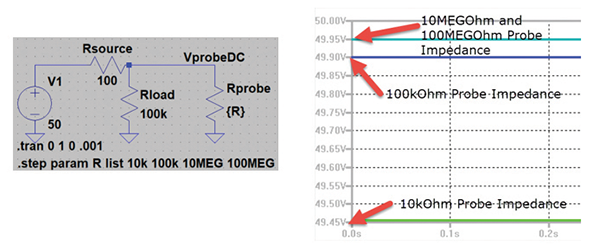
Figure 8: (Left) The SPICE schematic, (Right) the DC loading effect
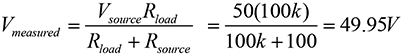
To explain this, we can turn to a simple SPICE example and our resistor divider example to form Figure 8 in SPICE. Before connecting the probe to the voltage divider, the voltage source is divided across the sources internal resistance and the load that the source is driving. This results in a voltage across the load calculated below:
Next, a probe is attached to the circuit placing another resistance in parallel with the load. Here we can use SPICE to simulate three different probe tip resistances, 10k, 100k, 1M, 10M.
We can see that, as the probe resistance increases, the effect on the dynamic measurement range becomes negligible and therefore we see most manufacturers’ probes specified at 1MΩ or above. DC Source loading affecting the dynamic resistance of your measurement is why probe manufacturers control the probe tip resistances, are often in megaohm range and offer attenuation switches.
AC Source Loading
When examining the loading effect of a probe at AC by adding in the two reactive components, the input capacitance and ground clip inductance, it is best to take them one at a time by first focusing on the probe tip capacitance.
This capacitance will have reactance that scales with frequency and, at low frequency measurements, it is noticed that the impedance of that capacitor acts as an open circuit offering little or no effect to the signal. It is at higher frequencies that this effect is more pronounced, making it common in situations such as measuring the rising edge of a clock trace.
To illustrate the effects of capacitive loading, a model of pulse generator driving a RC filter is introduced in Figure 9. We can simplify the circuit since the large impedance offered by the probe won’t affect the source resistance of the source, and because of the parallel capacitance that is added to the filter.
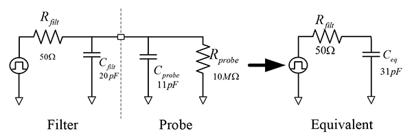
Figure 9: A probe connected to a RC circuit
Figure 10 demonstrates the effects as the rise times are affected by simply measuring the filter response.
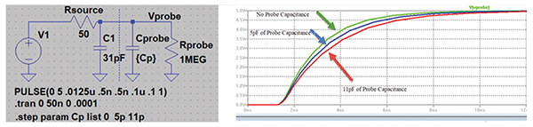
Figure 10: (Left) The SPICE schematic, (Right) the AC loading effect
Situations where the capacitance of the probe affects the signal are not limited to RC filtering but can be expanded to include:
- Antenna measurement where the capacitance (and inductance) can change the impedance of the antenna circuit, this occurs with NFC applications; and
- Oscillator measurement where the capacitance can prevent an oscillator from starting.
For passive probes, it is a general rule that the higher the attenuation ratio, the lower the tip capacitance, and this effect scales with the number of probes connected to that point due to capacitances in parallel being additive.
Ground Lead Effects
As mentioned, the second physical characteristic that affects the measurement is the probe clip inductance; as a wire it has some amount of distributed inductance in the measurement loop. Shown in Figure 11, this inductance can form a resonant LC circuit which could result in ringing with only the input resistance of the probe for damping.
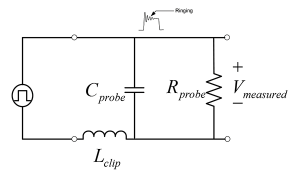
Figure 11: The ‘ground’ lead inductance in the probe model
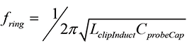
This resonant circuit will have a frequency response denoted by the ground lead inductance and probe tip capacitance, and is unavoidable but controllable. To understand what measurement frequencies that risk this effect, the transfer function can be worked out, resulting in the resonant point of the probe.
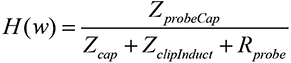
where
and
where
And an example of an AC response is shown in Figure 12 with a probe tip capacitance of 11pF and 60nH using a rule of about 20nH per inch (we are assuming a 3” ground clip). If we expand that to a time domain simulation of a square wave with various rise and fall times, we begin to see what I am sure many readers have been faced with in the past, ringing.
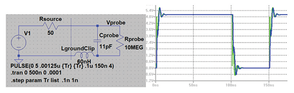
Figure 12: (Left) The SPICE schematic, (Right) the ground lead ringing effect
A simple test to see if the clip has a loading effect on the signal is to physically move the clip lead, as this changes the inductance associated with that leg of the current loop does. If the signal ringing you’re seeing changes, it is likely that your probe lead influences what you are seeing. It’s important to both:
- Utilize the hardware that comes with the probe such that the lowest inductance tip is always used; and
- The PCB designer take into effect probe clip test points which would direct the test engineer to the place resulting in the shortest loop to clip their probe to.
At some resonant frequencies with a 100 MHz oscilloscope, this ringing could be well above the bandwidth of the oscilloscope and may not be seen. But, with a faster oscilloscope, say 200 MHz, the ground lead induced ringing might very well be within the oscilloscope’s bandwidth and will be apparent on the display of the pulse.
Probe Effects on Amplitude, Phase and Bandwidth of the Signal
Now that a model of the probe has been established, it is important to analyze its effect on frequency components that make up the signal. Thus, it is important to consider loading effects at:
- The fundamental frequency;
- The frequency of the rise and fall time, typical many times greater than the fundamental frequency; and
- The upper harmonics of the signal being measured.
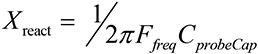
The overall effects on the amplitude and phase of the signal are determined by the total impedance at the probe, which is given by the resistive component and the reactive component, the latter being predominantly capacitive. The capacitive reactance scales inversely with frequency resulting in a low pass filtering effect manufacturers can use this information to chart impedance as a function of frequency in a datasheet.
If these do not exist, you can chart the reactance manually by using the following formula, which results in the reactance at the calculated frequency:
Typically, for a linear measurement, you want a constant magnitude and phase out to the frequency of interest; often you will find that probe manufacturers compensate by carefully controlling the probe resistance and any reactive elements inside of the probe (akin to tuning an antenna).
To see how the probe affects the overall bandwidth of the measurement, it is important to first take into account that there is a difference in both the oscilloscope bandwidth and the probe tip bandwidth. The oscilloscope bandwidth should be chosen such that it exceeds the frequencies of signals of interest, while the probe tip bandwidth should match that of the oscilloscope, the more cost effective and controllable of the two being the probe tip bandwidth. As a rule, the probe bandwidth should always be equal to or exceed the bandwidth of the oscilloscope, as using a probe of lesser bandwidth
will limit the measurement by slowing the rise/fall of the signal.
To evaluate the bandwidth of the circuit probe, manufacturers offer the following circuit which can be mimicked in your own test setup, which utilizes a pulse generator set for a known rise time, in this example it is 1ns. The complete setup is shown in Figure 13.
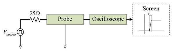
Figure 13: A factory test setup to test probe bandwidth
The test source is specified to 50ohm and terminated to 50 ohm. The rise time being measured is tied to the bandwidth of the oscilloscope and is defined as:
![]()
This results in a desired rise time of less than 3.5ns at 100MHz. Manufacturers provide standard accessories to deliver the specified probe and that most real-world signals are not 25ohm sources. However, this is a repeatable way to either verify whether the probe setup being used is acceptable in your application.
Now that the negative effects of the real-world probe model have been introduced, the obvious question to ask ourselves is what can be done to mitigate these effects?
Compensation and Probe Selection
Luckily, measurement device manufacturers have come to recognize the challenges of probing and have provided several ways to limit the negative effects brought on due to measurement. These come in two different forms:
- Choosing the right probe for your application to account for some of the drawbacks discussed in the previous section, as the goal is to select a probe that delivers the best representation of the signal to the oscilloscope for measurement; and
- Probe compensation, which allows you to match the probe capacitance to the oscilloscope input capacitance.
When choosing the appropriate measurement tool to connect to your oscilloscope, it is important to understand the options available such that the issues described are minimized. We first start this investigation by recognizing the wide variety of probes offered, and some criteria in how to choose them, then finish by understanding the tools available to tune that probe to the oscilloscope being used.
Understanding Probe Choices
There are a variety of probing options that manufacturers offer to best suit the application. To choose the most appropriate one to match the application, you must first recognize the signal source being measured. To do this, we can categorize signal sources to the following categories summarized in Figure 14, described as:
- Voltage signals – These are the most recognized types of probes and they come in two main categories, active and passive.
- Logic Signals – These are probably the second most utilized types of probe, which are active only probes as they must be low in probe capacitance to measure digital logic signals.
- Current Signals – These probes are categorized as active or passive probes, and are used as a sort of transducer to transform current to voltage.
- Others – Any probe that measures things such as temperature or vibration as voltage is described in this category.
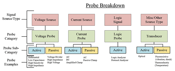
Figure 14: Breakdown of the various types of probes available
Therefore, to choose the best probe for your application it is best to first start with the type of source you are measuring. After understanding the source being measured, the next thing to take into consideration is the signal source impedance and bandwidth considerations, so as not to load down the source being measured. To probe requirements, it is important to remember:
- The probes’ impedance adds to the signal source, resulting in a new signal load impedance that affects the rise and fall time;
- In sensitive applications, such as measuring communication busses or clock signals, it’s important to keep the source impedance substantially greater than the source impedance to minimize the effect on the measured amplitude; and
- The probe capacitance scales inversely with the attenuation setting of some passive probes, and influences the rise and fall time of the signal being measured.
For voltage signals, an active, low capacitance probe is best in many applications as it offers low resistive loading and very low tip capacitance at the expense of dynamic range (and cost). To understand why an active probe is so desirable compared to a passive probe, the internals depict the differences between the two.
Passive versus Active: What’s the Difference?
In many different probing categories there are sub categories that further subdivide the category into active and passive type of probes. Passive probes are among the most commonly used probes for taking general purposes measurements, constructed sometimes with wire, connectors and a housing, along with compensation components they are rugged and generally inexpensive. The passive probe model is described in Figure 15, as it is connected to the cable and the input of the oscilloscope and looks like the model previously discussed.
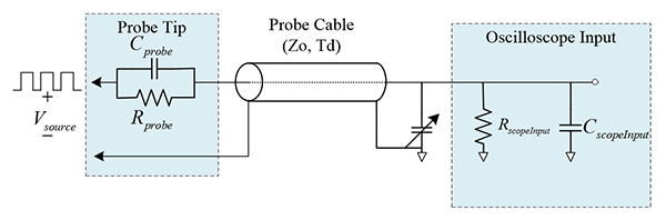
Figure 15: Passive probe model
They have no active components, and often have some sort of compensation mechanism to match the oscilloscope’s input.
Active probes, on the other hand, get their names from the fact that they contain active components such as FET based amplifier (as in the case of Figure 16).
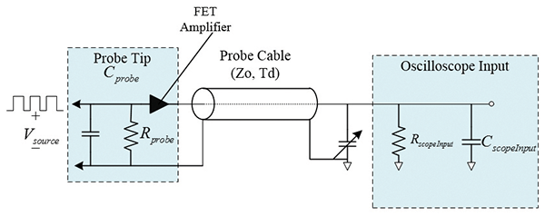
Figure 16: Active FET probe model
And a differential amplifier for differential measurements (as in the case of Figure 17).
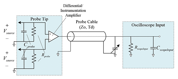
Figure 17: Active differential probe model
These are commonly used for high-speed, or high impedance measurements as the passive probe can cause noticeable circuit loading as their impedance is not significantly higher than the source they’re measuring. Active probes employ amplifiers, with some sort of transistor input which offers extremely high input impedance along with low capacitance at the drawback of being expensive and the need for them to be externally powered.
Probe Compensation
While there are a variety of probes to choose from, engineers will almost always be faced with a standard voltage-based probe multiple times in their careers. It is important to understand that many of these probes offer compensation via a (often-ignored) set screw on the housing, as these probes need to match the input capacitance and resistance to that of the oscilloscope to which they are connected. To further understand this, the probe model in Figure 18 is expanded to include the probe, probe body, the probe cable, an optional tuning box and the oscilloscope input.
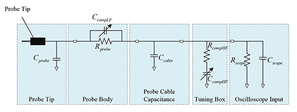
Figure 18: The complete passive probe model with the probe body and tuning box capacitors
It is important to notice that there are two methods for compensation:
- Low Frequency (LF) compensation, which involves tuning the frequency response of the x10 probe in the lower kHz region by tuning the set screw on the probe body itself; and
- High Frequency (HF) compensation, not all probes have, exists is in the tuning box part of the probe and is represented by CcompHF and RcompHF.
To understand what turning that screw does, we direct our attention to the probe body. For example, we see the probe input impedance at 9MΩ, which when paired with the input impedance of a 1MΩ oscilloscope gives 10MΩ overall impedance. This is meant to isolate the cable and probe from the device. In parallel we see a variable capacitor, CcompLF which forms the low frequency tuning section of the probe. It serves to match the time constant described earlier, formed by the probe, to the time constant formed by the capacitance of the oscilloscope and cable along with the resistance of oscilloscope. If we look at just these components at AC and DC, we see that at DC we have a resistor divider formed between the probe and oscilloscope and a capacitor divider at AC.
The best way to tune this is to input a square wave with a known edge that is within the bandwidth of the measurement system and without overshoot. Then, as you turn the set screw, you should see one of three situations happen described in Figure 19.
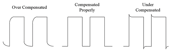
Figure 19: (Left) Over compensated probe, (Middle) a compensated probe, (Right) an under compensated probe
Most probes are compensated to the oscilloscope they are meant to connect to, but it is up to the engineer to compensate those probes when swapped to different measurement devices.
While most probes have a LF compensation part, others have an additional set screw on the part that connects to the oscilloscope. This allows tuning at HF, or very HF, by allowing the engineer to account for the parasitic effects of the cable impedance and the input impedance of the oscilloscope. The HF tuning section of the circuit attempts to shunt the input of the oscilloscope with a small capacitance and series resistor at the BNC connector. The HF compensation part represents RcompHF , CcompHF in Figure 18 and is tuned in similar fashion to the LF part, by utilizing a signal generator with a very fast edge and little to no overshoot. This circuit functions by allowing high frequency harmonics a low input impedance path away from the oscilloscope input, resulting in them not affecting the measurement.
Conclusions About Real World Probing Effects
Probe effects, either due to source loading, too much capacitance filtering the signal or excessive ground leads all leading to specific negative effects. Fortunately, solving these issues is possible through a combination of:
- Improving measurement techniques using test points indicating where to connect the ground clip (for a short loop) and utilizing associated probing hardware;
- Choosing the right probe that matches your oscilloscope manufacturer’s recommendations and application, which often means ditching the alligator coax or grapple connectors and looking for a probe; and
- Compensating a new probe to the oscilloscope input being used by the probe.
By understanding these concepts and the various parasitic effects the probe can have on the signal, the next time someone goes for some alligator clips to measure your clock signal, you can stop them and remind them that “an engineer is only as good as their measurement device!”
 Christopher Semanson works at Renesas Electronics America Inc. as an Electrical Applications Engineer in Durham, NC supporting a wide variety of general purpose applications. He has five years previous experience in EMC Education at the University Of Michigan, teaching EMC and Electronics with Mark Steffka. He has a bachelor’s degree in Electrical and Computer Engineering and a master’s degree in Electrical Engineering from the University of Michigan Dearborn. Chris can be reached at christopher.semanson@renesas.com.