
Conducting System-level ESD Current
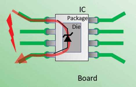
A previous article (Challenges of Designing System-Level ESD Protection at the IC Level: Misconceptions Regarding Current Flow to the IC [1]) highlighted the challenges an IC designer faces when trying to determine the actual current that will flow into the IC during system-level ESD exposure. Once the current magnitude, duration, and wave shape reaching the IC are established, the next challenge can be addressed—properly designing for the current to flow through the IC, without impacting the system performance. As shown in Figure 1, this requires allowing the system-level current to flow through the board and the IC (both the IC package and die).
It is a common misconception that designing an IC for system-level ESD requirements simply requires an increase in the capability of the ESD cells, which are already present for safe handling ESD requirements, like Human Body Model (HBM). While creating an ESD cell that can conduct system-level ESD current is certainly not a trivial task, there are other significant challenges that must also be addressed. This article will discuss three of those challenges. First, the system-level ESD currents and current rise times are significantly more severe than those for safe-handling ESD requirements— as a result voltage drops across the circuit interconnects are much more difficult to manage. Second, the IC is connected to a full system during the stress; other components are attached to the IC, and these components can affect how the current returns to the system ground reference during the ESD event. Finally, system-level ESD is typically applied to a system that is powered up and operating, with more stringent failure criteria than those for safe-handling ESD requirements. While each of these challenges is significant by itself, this article will show how these challenges impact one another, further compounding the difficulty of meeting the system-level ESD design requirements.
As ESD current flows through a circuit path, additional voltage drops occur because of the impedance of the conductors which connect the circuit elements together. Typically, these impedances are small enough to be easily managed or even ignored. But consider a case where an IC is expected to conduct an entire system-level ESD event, produced with a 150 pF, 330 Ohm RC network [2].
When discharged at a typical 8 kV requirement, in contact mode, this event produces the current waveform shown in Figure 2. This current waveform has an initial peak current of 30 Amps, followed by a second peak current of 18 Amps. The initial rise-time and peak-current combine to produce a dI/dt of 3.75 E10 Amps per second. These values are much higher than typically experienced in normal operation, and even in safe-handling ESD conditions, requiring much lower impedances. The entire impedance in the system-level ESD current path must be considered—this includes the IC interconnect (both the metal routing on the die and the package interconnect and bond wires) and the board-level routing. Voltage excursions of tens of volts can arise from resistances as low as one-half of an Ohm and inductances as low as a few hundred pico-Henries. If system-level ESD protection is part of the IC, the designer must carefully consider where these protection elements will be placed on the die and optimize both the resistance and the inductance of the interconnect. The impedance requirements can be so low that extracting and predicting them (based on the geometry of the interconnects) can be as significant a challenge as actually achieving them.

In a safe-handling ESD test, like HBM, a single pin is stressed with respect to another pin (or group of pins) while the other pins are left floating. This allows the IC designer to clearly identify where current will enter and exit the IC. For system-level ESD testing, the IC is exposed while connected to the entire system—and, while the point where current enters the IC may be clearly identified, the exit point for the current is not clear. Circuitry on the die can connect to external circuitry in the full system in such a way that unexpected (and non-trivial) current paths are completed. This creates an added challenge for the IC designer, who must now consider how the IC interacts with the system, during system-level stress.
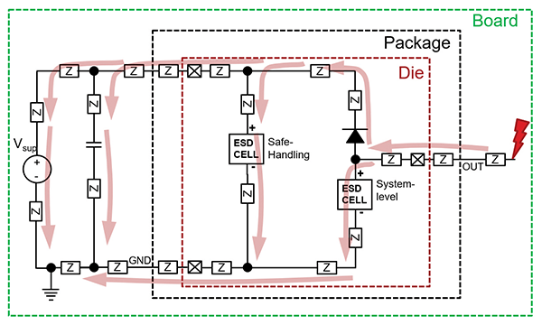
Here is a simple example of how unintended paths can be created. A common scenario is for an IC pin to have a diode on the die between an output pin and the power supply, connected in such a way that the diode is forward-biased when the output voltage exceeds the power supply. This diode may be part of the ESD protection strategy or may be part of the IC circuitry. Figure 3 shows an example of a case where the IC designer intended for the system-level ESD current to be conducted by an ESD cell directly between the output pin and ground, but a diode also exists between the output pin and power supply. When positive system-level ESD current is injected into the output pin, some of that current can flow onto the power supply net, and from there it can flow back to ground, either through the power supply’s ESD cell or out of the power supply pin and flow through decoupling capacitance or power supply in the actual system. Each of these paths must be considered and optimized to ensure they can carry the necessary current. But how current is shared among parallel paths is dependent on the impedance; this second challenge is thus exacerbated by the first challenge—parallel current paths exist, and determining their relative current requires careful consideration of the interconnect impedances.
The third challenge the IC designer faces is the fact that system-level ESD is often performed with the system powered-up and operating. Because the IC is powered, there is risk of a latch-up event being triggered by the ESD event—a risk which is not present in safe-handling testing. In addition to this risk, there is added consequence of a powered, operating system—if changes in how the system operates occur during or after the application of the ESD event occur, this may be deemed a failure. Each system has its own requirements for determining pass or fail, and the IC designer must understand these requirements and design for them. Designing the IC to avoid disruptions can be a significant challenge. Imagine a signal that is driven to 3V relative to a 0V ground reference, an input circuit sensing that signal, whose ground reference is at 3V, will not interpret that signal correctly. Thus, if the ground bus of the IC (or the system bus between two components) encounters voltage drops during the ESD stress, unwanted logic changes can occur, causing disruptions to the normal operation. For example, a logic change in a power-on-reset circuit could initiate a reset of the IC, significantly disrupting the operation of the full system. Managing the interconnect impedances and the relative current flow in parallel paths are significant challenges, just from the perspective of conducting the ESD event without physical damage. The added constraint of avoiding disruptions to normal operation adds significant complexity to the design.
This article has discussed three significant design challenges that result when system-level ESD protection is integrated into and existing IC. While the marketing advantages of such integration are well established, the engineering challenges are real, and must be carefully considered by the IC designer, within the full context of the overall system design. The challenges are more significant than simply sizing an existing IC-level safe-handling ESD solution to conduct the higher system-level ESD currents.
References
- H. Kunz, “Challenges of Designing System-level ESD Protection at the IC-level: Misconceptions Regarding Current Flow to the IC,” In Compliance Magazine, August 2022.
- Electromagnetic Compatibility; Part 4-2: Testing and measurement techniques—Electrostatic discharge, IEC 61000-4-2, edition 2; 2008