
The equipment should have passed the emissions scan. It should not be susceptible to this noise. The filter analysis said this was not a problem. The case should be an excellent shield. Why doesn’t this pass?
There are two statements I have heard about electromagnetic interference which are both related and true: EMC is the science and engineering of things that are typically not on the schematic [1], and EMI is often caused by issues of geometry [2]. The first statement speaks to the issues of parasitics, or cross coupling of energy due to magnetic induction or capacitance. The second says that the parasitics can be controlled or reduced if the proper routings and separations are maintained, and that once a degree of understanding about these coupling mechanisms is understood the control of them can be obtained.
Rules of thumb are dangerous in this field. Yes, there are some concepts that often work. But there can be so many variables that create these problems, that using only “rules of thumb” can lead you down the wrong path or not explain the reason the issue exists.
However, much of what will be stated is based on these general rules. They may often work. They may not. To coin a phrase we, as consultants, often use, “It depends”. But hopefully they can inform, instruct and help you to avoid the issues stated earlier. So here, rules of thumb will be avoided but not totally ignored.
General Concepts
It is important to remember how these energies move around and cause problems. First consider the concept of common mode energy. Common mode energy, or CM, is energy which moves on two or more wires in the same direction and in phase. It is quite different from differential mode energy, which travels in opposite directions on adjacent wires. An input power line and power return line are a differential mode pair – the currents on one travelling in the opposite direction from the other.
Common mode energy may also exist on that same pair of power line wires. The source may be from an inductor or transformer located near the lines inside the unit (inductive coupling), from the circuit board power plane voltage which may be driven with respect to the chassis (a form of conducted coupling), or from a high voltage source, maybe a heat sink, located near these lines (capacitive coupling). It can also be coupled onto these lines outside the equipment from various sources, either radiated onto the lines (radiated coupling), or capacitively or inductively coupled onto the lines, as performed during conducted immunity/susceptibility testing.
In each of these cases, the energy on these lines is found to be common mode – energy induced on both or all lines at the same time and in phase.
When I was in college, my professor wrote on the board the following formula:
L = L1 + L2 ± 2M12
where L is the total inductance of a wire loop from source to load and back, L1 is the inductance in the first wire from the source to the load, L2 is the inductance in the second wire from the load back to the source, and M12 is the mutual inductance between the wires, which is doubled because each wire has the same effect on the adjacent wire. But the equation is ± 2M12. Yes, plus or minus. The question is, when is the formula + M12, and when is it – M12?
Without using names like “Maxwell”, which tends to just detune the reader from any further input, it must be noted that when you move an electron, it creates a magnetic field. This is the basis for inductance. In a wire, we move a bunch of electrons, creating a bunch of magnetic field. If a second wire is nearby, this bunch of magnetic field wants to generate a current in the wire in the opposite direction. This is mutual inductance “M”. This is how transformers work. But assume that the other wire already has current in it in the opposite direction. Then there is a beneficial arrangement and the induced magnetic fields in each wire end up assisting the adjacent wire, which is a “reduced impedance”. Then the formula uses – M12.
But what about common mode noise? Well, common mode energy is routed in both wires together and in the same direction in phase. This means that the induced currents in each wire do not benefit but oppose each other, and this ends up increasing the overall inductance. Then the formula uses + M12.
This whole concept is part of the reason why twisted wires work so well. Twisted wires have a mutual affinity to differential energy over common mode energy. The same concept works with traces over ground planes. As long as a clock or data trace is routed over a single plane and does not pass over any cut in that plane, and the return current is referenced to that same plane, then the return path will couple directly under that trace. This reduces the trace impedance, and also the loop area between the signal and return, resulting in much lower radiated emissions and higher immunity to external energy interfering with the signals. This works for frequencies above 100 kHz.
Now all this talk about wire inductance brings up another concept: wires do not make good RF grounds. This is true if you are using a wire to try to conduct noise to some type of grounded structure or using a pig tail to terminate a shield. Shielded cables terminated into a pigtail tend to have several issues. They are inductive and thus have high impedance. They carry a current that generates a magnetic field which can couple energy into the adjacent lines they are trying to shield. Suffice it to say that it is best to use a symmetric termination of the shield, if not a full 360 degree termination at the connector.
As for using a wire to ground out a noise source: first remember that currents flow in complete circuits. If there is a current flowing in that wire, it has to be returning to the source by some other path. The farther away that path is, the larger the loop, and therefore the higher the inductance of that path. There are no RF sinks or holes that you can pour the noise into. But there may be a good deal of induced currents on the chassis from inductive and capacitive circuits, and those currents must find a path back to the source. Several low impedance paths are always best and, again, symmetry is desirable.
Finally, what is low impedance? Lower than you have now, otherwise you likely would not be reading this article to begin with. The “rule of thumb” used for a long time was that 2.5 mΩ was the required bonding resistance for chassis, connectors, and other metal to metal contacts. Your mileage may vary, but this might be a good goal to strive for. And in case you were wondering, 4½ inches of 18 gauge wire is 2.5 mΩ, not including the minimum 0.15 µH of inductance (depending on return path inductance, loop area and so forth, and 0.15 µH is about 1 Ω at 1 MHz, so that won’t work very well at all…).
Emissions Issues
Please note that radiated emissions energy is likely due to common mode energy on the wires. Why? First, common mode energy radiates much more effectively than differential mode energy. Many formulas state the level is effectively about 106 or 120 dB more. Also, since the typical wavelengths for most radiated emissions found are rather long, the types of antennas needed to transmit these must also be significant in size. Remember that at 300 MHz, a wavelength is about 1 meter. At 100 MHz it is 3 meters. The ratio between frequency and wavelength is linear in this regard. Also, for something to radiate well at lower frequencies, it may need to be physically long or large. This does not mean you can’t have a small object radiate at low frequency, only that if you place a long wire on the small object which is tied to the noise source, it will likely radiate much better.
So if the radiated emissions are below about 200 MHz, first check the cables. Are the cables filtered? Are there shields used? And if they are, are the shields well terminated at BOTH ends? The first argument against grounding a cable at both ends is that it causes ground loops. Unless you are a guitar player who gets 60 Hz hum in the sound system, why are you worried about ground loops? It is rare that the shield grounded at both ends causes more problems than it cures.
Also, if performing commercial testing, it may be found that emissions below 80 MHz or so are vertically polarized and the antenna is at the lowest point on the mast. One issue to look for is the amount of capacitance the equipment has to the ground plane. Is there a power cord draped across the ground plane? Are there cables which are hanging down to the ground plane? Is this floor standing equipment where you typically have the unit isolated from a ground plane, but now it is resting directly on the conductive surface? These issues can create a capacitive coupling network which can couple back to the antenna. Remember that broadband antenna, vertically polarized and at the bottom of the mast, have much higher capacitance to the ground plane than, say, a dipole antenna (Figure 1).

Figure 1: Radiated emissions vertically polarized antennas
In the top drawing, a broadband antenna is used to measure radiated emissions; in the bottom, a tuned dipole. Note that the tuned dipole has less capacitance to the ground plane as compared to the broadband antenna. Also, due to the length, the minimum height for the dipole forces the center to be higher off the ground plane and thus less on-line with the EUT.
So how did that noise get on the cables? First, every line which is routed in and out of the equipment must somehow be filtered or very well shielded. Every line that penetrates the enclosure of the equipment must be treated as a noise carrying device. It does not matter what the wire does – whether it is an input or an output; whether it carries hundreds of amperes of current or a microampere at a microvolt. The presence of a conductor routed from near noise generating circuits to a location away from those generators can carry radio frequency energy down the cable, where it radiates back to the source. Unfortunately the test laboratory puts an antenna in the return path, and then reports the results in unkind terms.
Second, when a filter is used, the location of the filter is critical. In order to have the best results, filters must be placed near the point of penetration in or out of the equipment. When a filter is placed inboard and away from the connector, radio frequency energy can cross couple and contaminate the filtered lines. In Figure 2 and Figure 3, the effects of filter placement are seen. In these two graphs, the filter component and the essential layout was the same. Only the location of the filter was moved, from about 6 inches from the connector to the edge of the board by the connector.
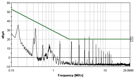
Figure 2: Filter location inboard of equipment

Figure 3: Filter location near the equipment connector
Components
So what types of components make a good filter? Capacitors should be the first line of defense. They are inexpensive and can be relatively small and light weight. But there are many reasons that capacitors do not work. The most obvious is the value or size of the capacitor. For lines which do not carry clock or data signals, the capacitor can be large … or as large as practical. However, on data and clock lines, care must be taken not to filter the signal. Thus the value must be carefully chosen to maintain the data frequency and five to ten harmonics of the signal.
Another issue with capacitors is the type of capacitor used. Electrolytic capacitors provide high capacitance per volume, albeit polarized and therefore not useful for AC. However, they tend to have high equivalent series resistance (ESR) and may have high equivalent series inductance (ESL) as well. This limits the useful frequency range to 100 kHz or so. For this reason, ceramic capacitors are often used for high frequency applications. And yet…
Issues of lead inductance, trace inductance and routing, inductive cross coupling, and other issues are common with the use of capacitors. Designs can be careful to assure the circuit has very short traces to the decoupling capacitor, and then disregard how the return side of the capacitor gets the energy back to the source. The entire loop from the source to the capacitor and back to the source must be analyzed and verified. Too often circuit designs rely on a ground symbol to dump the noise into, and then ignore how that symbol connects to the same symbol on the noise source. To make a point that the layout engineer should know where the return traces should go, and avoid an Auto Routing feature, the consultant would use the symbol shown in Figure 4.
Figure 4: “No Ground” symbol
It should be pointed out that the purpose of a capacitor is to bypass RF currents and return them to the source of the noise. However, the process of doing so can in itself create issues. Consider Figure 5, which shows how a capacitor passes these currents back to the return path. However, if the leads on the capacitor are long, or if the traces to the capacitor are long, this can create a source of inductive coupling. And if that coupling is in the loop that is trying to be filtered, the whole process ends up bypassing the filter. Admittedly, this is a lossy system, and there is benefit to the capacitor. But consider how much better the results might be in a setup using current routings seen in the lower drawing.

Figure 5: Capacitor cross coupling
Another issue often missed is the presence of a DC bias on a capacitor. When a voltage is placed on a capacitor, the total available capacitance is reduced. In Figure 6, the presence of a DC bias voltage on a capacitor rated for 16 VDC is shown. The higher the voltage placed on the capacitor, the less capacitance will be found. This is more true for the very small format capacitors, e.g. 0603, 0402, and so forth. Looking at Figure 6, note the effect on the 0402 format as compared to the larger 0805 format. If an 8 VDC bias is placed on these capacitors, the 0805 will still have 93% of the rated capacitance, whereas the 0402 is down to 22% – a 12 dB change in value (based on a 20Log system).
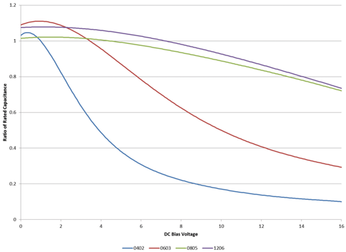
Figure 6: How DC bias voltage effects capacitance
Ferrites are very commonly used in EMI control. However, how they are used and where to use them is often a mystery.
It should be understood that ferrite core inductors are somewhat different than standard inductors. A common inductor is a reactive device that creates an impedance mainly though the creation of magnetic fields, up to a frequency where the capacitance of the windings become dominant and start to reduce its effectiveness. The core material for these inductors tends to include nickel, iron, and possibly molybdenum or other materials. They have permeability which is relatively low, typically below 100. However they are designed to work with significant current and not suffer from “saturation”, an effect where the core cannot accept any more magnetic flux.
Ferrites work in a similar way at low frequency. However, as frequency increases, a ferrite becomes lossy and begins to have a resistive aspect. In Figure 7, a high frequency ferrite is analyzed for its impedance over frequency. The sloping line from lower left to upper right is the impedance with a single turn (no wraps) though a bead. The horizontal line shown in two steps is the phase of the signal. Starting at the right, the signal is at +90 degrees, indicating the inductance of the ferrite (ignore the noise, which is due to the measurement limits of the impedance analyzer). Note that at 10 MHz the phase makes a step down to 60 degrees, indicating a resistive nature is being introduced.
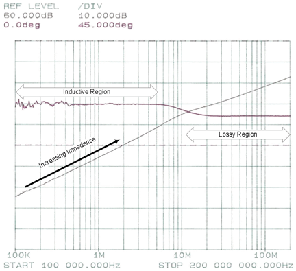
Figure 7: High frequency ferrite characteristics
This particular “high frequency” ferrite has a nickel zinc, or NiZn, formulation with a ferrous oxide. These ferrites are commonly used for most commercial radiated emissions and susceptibility control. A characteristic of NiZn ferrite is that the permeability of the material is typically less than 1000, and for very high frequency material may be less than 125.
The other common ferrite material is mangnese zinc, or MnZn, again formulated with a ferrous oxide. These cores can have high permeability, typically over 1000. However, with the high permeability comes a reduced bandwidth of usefulness. So MnZn ferrites are best used for conducted emissions and susceptibility problems.
Note that ferrites can become saturated with less current than many inductors. The best use for ferrites is to use them common mode, on all lines with all return currents routed in the same core. In this regard, the core would be an impedance mainly for the common mode aspect of the noise, while allowing the differential mode noise to pass through with minimal impedance. See Figure 8 for how most differential mode energy is canceled inside a common mode wound toroid, and Figure 9 for how common mode energy increases inside the same toroid.

Figure 8: Differential mode fields in a common mode core
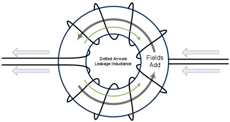
Figure 9: Common mode fields in a common mode core
The layout of the above toroids is often best when used on power lines, where spacing adds isolation which may be needed for safety concerns. However, if a common mode inductor is needed for a data line, the separation of these wires may create issues with respect to high frequency data transfer. In Figure 10, the windings are shown wrapped together, as would be required for data lines. Note that the additional benefit is that it reduces the leakage inductance found in the previous figures.

Figure 10: Common mode core wound for data signals
Shields
There is equipment in which the shielded case is so thick, it has “Two Man Lift” warnings on the cover, even though it is the size of a laptop. Yet I have seen these fail. Conversely, I have seen aluminum foil work to shield a unit with wide margins. Why does one work and the other not?
For radiated emissions, say above 30 MHz, a metal shield does not need to be thick. Aluminum foil has over 80 dB of shielding, and that is for both electric and magnetic fields. The conductivity of the metal makes a great reflective shield for the electric fields, while the magnetic fields are highly absorbed due to eddy current losses. So why is an enclosure that is made of heavy metal not a good shield?
Several things are involved in the breakdown of the shield. First are the cables and wires. Every wire that penetrates the shield must be filtered at that point. If it is not, then noise on the inside of the equipment can couple onto that line, and then transmit on the outside of the chassis. Likewise, during immunity/susceptibility testing, energy is coupled onto those lines and will be conducted into the unit. This must be shunted to chassis or impeded in some manner, otherwise susceptibility may be found. In this case, all the shielding in the world will not help to remove this coupling.
In the event that the filter is in place and is working well, a shield may break down at seams and joints. As stated earlier, bonding impedances of milliohms or less are needed to create a good bond. This is even more important at shields joints. The circuit inside the equipment will generate fields which will create currents on the metal structures, staying on the inside surface due to skin effects. These currents must be allowed to flow back to the source with minimal impedance. As long as the metal does not have joints, the current flows with micro-ohms of impedance. When a seam is crossed, an impedance may be thousands of times higher than one traveling to the outside of the shield, where it can radiate.
The solution is to assure the lowest possible impedance between any metal contacts. Wide and continuous contacts are best. This means that coatings and paint on metal surfaces must be masked at joints and seams. The type of coatings used must assure contact will be of the highest quality possible. And before you go to the lab for a test, make sure to put in all the mounting screws. Do not assume that one in each corner is good enough.
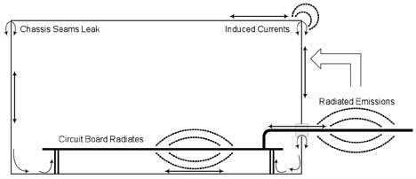
Figure 11: Shield currents
In Closing
This article is not intended to address every aspect of EMI issues; there are many books, papers, and week long lectures that can help. Instead, remember the following points:
- Follow the currents. Electromagnetic interference is based on currents, and currents must flow in a loop. There may be a displacement current involved (read: capacitance), but it is still a current. Success depends on allowing those currents to flow back to the source.
- Assure local returns. The closer to the source these currents return to the source, the less emission and susceptibility you will find.
- Keep impedances low for return currents. Enough said.
- Remember parasitics. Most of these issues are caused by cross coupled noise in some regard. The cause did not appear on your schematic. So look to see how it might be cross coupled.
- Remember the geometries. Loops of wires and thus currents both radiate and will be susceptible to radiation. Keep the loops small. Return currents with the signals as close as possible.
There are many other such items that could be noted. But basically, many are just “rules of thumb”. ![]()
Notes
- Stated by Chris Kendall among others
- Stated by Dr. Tom Van Doren among others
 |
Patrick G. André received his physics degree in 1982 from Seattle University. He has worked in the electromagnetic compatibility (EMC) field for 30 years. Patrick is an iNARTE Master Design Engineer and a Certified Engineer in both EMC and ESD. He has worked in the military and aerospace environment for his entire 30 years career, and worked in the commercial electronics environment for the last 20. Patrick has a strong ability in both the test and measurement and troubleshooting areas of EMC. He is president of André Consulting, Incorporated. Patrick has been a member of the IEEE EMC Society for 29 years, serving as chairman, vice chairman and arrangements chairman of the Puget Sound Section. He also works for the Seattle Gilbert and Sullivan Society as a Sound Design Engineer and Photographer. Patrick can be contacted at pat@andreconsulting.com or through http://andreconsulting.com. |
