In earlier articles in this publication we have discussed the charged device model (CDM) testing of small devices. In the first article we demonstrated that the peak current for small devices does not become vanishingly small.1 The commonly held belief of vanishing current for small devices was shown to be an artifact of measuring the current with the 1 GHz oscilloscope2 specified in the JEDEC CDM standard.6 The second article explained various ways to make CDM testing of small devices more reliable with the use of small surrogate packages, or the use of templates to hold the device during testing.3 In this article we will show how insight can be gained into the CDM testing of small devices using a simple three capacitor circuit model.4, 5
The CDM Test
A diagram of a CDM tester built to the JEDEC field induced CDM standard6 is shown in Figure 1. The tester consists of a Field Plate, whose potential can be controlled by a high voltage power supply through a high value resistor. Above the Field Plate is a Ground Plane. At the center of the Ground Plane is a pogo pin. The pogo pin is connected to the Field Plate with a disk shaped 1 Ω resistor as well as to an oscilloscope through a 50 Ω cable. The Ground Plane can move in three dimensions relative to the Field Plate such that the pogo pin can be made to contact the pins of an integrated circuit placed pins up on the Field Plate. To perform the test, the device under test (DUT) is placed on top of a thin insulator on the Field Plate. The potential of the Field Plate is then slowly raised to a high voltage, 500 V for example. Since the capacitance between the DUT and the Field Plate is much larger than the capacitance to anything else, the DUT potential will closely track the Field Plate potential. To perform the actual stress the Ground Plane is moved such that the pogo pin touches a pin of the DUT. This quickly grounds the DUT, resulting in a very fast current pulse between the DUT and the pogo pin. The oscilloscope measures the CDM current pulse by sensing the voltage across the 1 Ω resistor. Sample CDM waveforms are shown in Figure 2 for the small and large modules specified in the JEDEC CDM standard to calibrate CDM testers. These modules consist of small metal coins of a specified size and capacitance to the Field Plate.
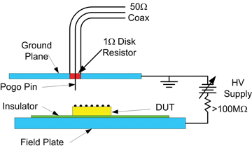
Figure 1: Diagram of a field induced CDM tester according to the JEDEC CDM standard
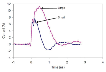
Figure 2: Measurements of the small and large JEDEC calibration modules using an 8 GHz oscilloscope
Circuit Model
The above explanation of how a field induced CDM test is performed does not show what controls the magnitude and time dependence of a CDM event. To do this a circuit model is useful and a simple one is shown in Figure 3. CDUT is the capacitance between the DUT and the Field Plate, CDG is the capacitance between the DUT and the Ground Plane and CFG is the capacitance between the Field Plate and the Ground Plane. The resistance between the pogo pin and the Ground Plane is the 1 Ω current sensor. The 50 Ω resistance of the oscilloscope is ignored. The resistance of the spark which forms between the pogo pin and the DUT is assumed to be a simple resistor. The inductance of the pogo pin and spark are lumped as a single inductor. The values of the spark resistance and the inductance will be used as fitting parameters. This model is the same as that proposed by Montoya and Maloney4 and the 3 capacitor model of Atwood et al.5 Atwood has also proposed a 5 capacitor model, which includes capacitance between the Field Plate and Ground Plane to the CDM tester’s chassis, which is more accurate, especially for large size DUTs and long times. For small devices and short times the 3 capacitor model is very informative as we shall see.
The circuit in Figure 3 was implemented in the Spice simulator LTSpice.7 The Spice circuit diagram, with values used to simulate the large JEDEC calibration module, is shown in Figure 4. A voltage controlled switch is used to represent the spark as the pogo pin approaches the DUT pin. A switch resistance of 26 ohms represents the resistance of the arc. The voltage source V2 is used to trigger the switch and was set to trigger the switch at 1 ns. The voltage source VCDM provides the test voltage, 500 V in the simulations presented. A 9 nH inductor represents the combined inductance of the spark and the pogo pin as well as a small ferrite bead included in the Ground Plane assembly to tune the waveform to match the JEDEC standard. The values for CDUT are from parallel plate calculations and are very close to the nominal values in the JEDEC CDM standard. CDG is calculated assuming a parallel plate capacitor and a 3 mm long pogo pin. The value of CFG is also based on a parallel plate capacitor model with a peripheral capacitance term minus a capacitance representing a shielding of the Field Plate to ground plane capacitance due to the size of the device under test. The separation between the Field Plate and the Ground Plane was equal to the 3 mm long pogo pin and the thickness of the JEDEC calibration module. The capacitance values used are shown in Table 1. In the simulation the potential of the DUT is set to an initial condition expected for the midpoint between two capacitors in series with a voltage across them, in this case 487 V.
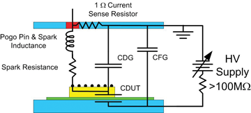
Figure 3: CDM setup with superimposed circuit diagram
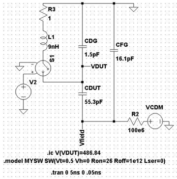
Figure 4: Spice implementation of 3 capacitor CDM model
| Parameter | Large JEDEC | Small JEDEC |
| Diameter (mm) | 25.4 | 8.89 |
| DUT to Field C | 55.3 pF | 6.78 pF |
| DUT to Ground C | 1.5 pF | 0.183 pF |
| Field to Ground C | 16.1 pF | 17.0 pF |
Table 1: Values used in simulations
Comparisons of the measured and simulated CDM waveforms are shown in Figure 5. The measured data is the same as shown in Figure 2. There are two major features of interest beyond the good agreement between the simulations and the measured data. First of all, the peak current drops only by about 25% even though the DUT capacitance values differ by a factor of 2.9. The second feature is that the width of the major peak is much narrower for the small module. This shows that the narrower pulse widths for small DUTs shown in the first article in this series1 is simply a property of the LRC circuit which makes up the CDM tester.
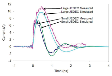
Figure 5: Comparison of measured and simulated waveforms for the JEDEC calibration modules
The voltage on the DUT and the Field Plate during the CDM event helps in the understanding of what occurs during a field induced CDM test. Figure 6 shows a plot of the current into the DUT, as well as the voltage on the DUT and Field Plate for the simulation of the large JEDEC CDM module. The simulated current is the same as that shown in Figure 5. The voltage on the DUT starts at just below 500 V, as discussed above, and then falls quickly to zero volts with a small oscillation. This result is what would be expected for the rapid grounding of the DUT. What is often less appreciated is what occurs to the voltage on the Field Plate. The Field Plate voltage drops to a value just over 100 V after a small oscillation. This shows that the CDM event consists of a rapid movement of charge between the three capacitors in the model, with the main movement of charge being from CFG to CDUT. The charge movement is dominated by the CDUT and CFG capacitors due to their larger size. The voltage on the Field Plate will only rise back to 500 V with a time constant in excess of 1 ms due to the large resistor between the Field Plate and the power supply.
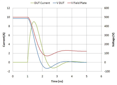
Figure 6: Current and voltages for a simulation of a CDM event for the large JEDEC module
Discussion
The simulations shown here provide useful insight into the field induced CDM test. The event is a rapid movement of charge between the capacitances of the field induced CDM tester. The geometry of the test fixture is critical in terms of determining the capacitance, especially CFG. CFG is affected by many things besides the dimensions of the Ground Plane. The length of the pogo pin and the thickness of the DUT are obvious. Calibration of the CDM system is performed using coin shaped modules with a thickness of 1.27 mm. Many integrated circuit packages such as Pin Grip Arrays are much thicker than this. The thickness of a product when tested on the CDM machine will therefore affect the severity of the test it receives due to changes in the Field Plate to Ground Plane spacing. The area of the DUT will also affect the value of CFG. As the DUT size, and therefore capacitance, increases it will shield a larger area of the Field Plate resulting in a decrease in the value of CFG. The result is that as DUT area and capacitance increases, CFG decreases. This enhances the well known property of CDM stress not being linear for large DUT capacitance.
The values of pogo pin, spark inductance and the spark resistance are not precisely known values, which limits the ability of the circuit models to be used as predictive tools. Spark length and resistance is an area that could be a science in itself. Spark properties depend strongly on humidity as well as the shapes of both the pogo pin tip and the geometry of the integrated circuit pin being tested. In the current analysis these values can be considered fitting parameters.
Conclusions
Circuit model simulations of field induced CDM measurements are a valuable tool in the understanding of CDM testing. They show how the event is a rapid movement of charge between the capacitances in the tester, and that the geometry of the tester, the properties of the device under test and properties of the spark are all critical to the severity of
the test. ![]()
- R. Ashton, M. Johnson, and S. Ward, “CDM Currents for Small Integrated Circuits,” IN Compliance, May 2010.
- M. Johnson, R. Ashton, and S. Ward, “FCDM Measurements of Small Devices,” EOS/ESD Symposium Proceedings 2009.
- M. Johnson, R. Ashton, and S. Ward, “CDM Testing of Small Integrated Circuits,” IN Compliance, June 2010.
- J. Montoya and T. Maloney, “Unifying Factor ESD Measurements and Component ESD Stress Testing,” EOS/ESD EOS-27, 2005.
- B.C. Atwood, et al., “Effect of Large Device Capacitance on FICDM Peak Current,” EOS/ESD EOS-29, 2007.
- JESD22-C101E, “Field-Induced Charged-Device Model Test Method for Electrostatic-Discharge-Withstand Thresholds of Microelectronic Components,” JEDEC Solid State Technology Association, December 2009.
- LTSpice is a product of Linear Technologies.
Robert Ashton joined the Discrete Products Division of ON Semiconductor as a Senior Protection and Compliance Specialist in 2007, having previously spent 3 years in the position of Director of Technology at White Mountain Labs, a provider of ESD and latch-up testing of integrated circuits. Prior to that, Robert was a Distinguished Member of Technical Staff at Agere Systems, Bell Labs Lucent Technology, and AT&T Bell Labs, in integrated circuit technology development. Robert has published numerous articles on ESD testing of integrated circuits, test structure use in integrated circuits and CMOS technology development, and has presented tutorials on ESD, latch-up, and Transmission Line Pulse testing at IEEE and ESD Association conferences. In addition, Robert is an active member of ESDA Working Group 5 for Device Standards, ESDA Working Group 14 for System Level Test as well as the JEDEC Committee 14.1 ESD and Latch-Up Working Groups and the IEEE Surge Protection Device Committee.
Robert received his B.S. and Ph.D. in Physics from the University of Rhode Island in Kinston, RI, USA in 1971 and 1977.
Marty Johnson returned to National Semiconductor in 2006 working in ESD device design debug and supervising the ESD Characterization Lab. He currently is supervisor of the ESD Qualification & Characterization Lab. From 2001 to 2006, he worked at Philips Electronics (Semiconductor Division) focusing on WLR and TLP characterization. During his tenure at Philips he was the corporate representative to the Reliability Technology Advisory Board (RTAB, now ISMI) and its chairman in 2004. From 1978 to 2001, he worked for National Semiconductor spanning the semiconductor reliability spectrum from basic reliability qualification through wafer level reliability to ESD and Latch-up. He is also active on the JEDEC ESD Team (JC-14.1), the Joint ESDA/JEDEC HBM and CDM teams and the JEDEC Latch-up Standards team.
Marty received his B.S. Physics from Midland Lutheran College in 1973, his M.S. Physics from the University of Tennessee Space Institute in 1975 and his M.S. in Electrical Engineering from the University of Nebraska in 1978.
Scott Ward joined Texas Instruments in 2007 to work in the field of device-level ESD testing and ESD testing standards development. He has since expanded his work to include factory ESD control and handling. Prior to Texas Instruments, Scott worked for Cypress Semiconductor in San Jose, CA. At Cypress, his work included ESD and Latch-up design and characterization; as well as device testing standards development. Since 2003, he has been a member of the ESDA Working Group 5 standards committee (device testing). Scott joined the JEDEC ESD standards task force in 2005. Scott is an ESDA member, attending every EOS/ESD Symposium since his first in 1996. Scott began his career at ZiLOG in 1995, designing on-chip ESD protection networks.
Scott has an M.S. in Electrical Engineering from the University of Idaho and a B.S. in Electrical Engineering from Montana State University.
