
Using Accessible Math and Computer Tools to Solve Heat Flow Problems
One early contributor to semiconductor ESD research was Jack Smith of Lockheed, who was fond of stating that all ESD damage is, in the end, thermal [1]. This is because there is always conversion of electrical field energy into heat, into mechanical motion of atoms. Even in the case of voltage overstress, field energy knocks atoms out of place at defect sites, thus linking field energy to the heat equation on a microscopic scale at least.
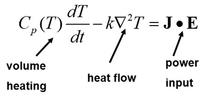
Jack liked to start a presentation on, say, metal heating with a universal equation (Figure 1) and go from there to specific cases.
In this article, our approach will be to examine some ESD heating cases where the analysis becomes simple enough to derive significant insight and overview, without necessarily going into an extensive calculation or computer simulation. Indeed, we’ll refer to some computer simulation work that was done with much-increased efficiency due to those insights.
The first thing to simplify in the general EOS/ESD equation is the 3-dimensional ∇2 term; we’d like to find effectively 1-dimensional (1-D) cases where that term becomes a double derivative, spatially. The power input for EOS/ESD is commonly some kind of I2R heating, so this is becoming manageable when we have a power input expression for a source at x=0.
Let’s say it’s an infinite planar source, units are per unit area. For 1D heating, the temperature of most interest in ESD is the highest, the surface temperature, a scalar number at the heat source, x=0. If there is a critical temperature for ESD failure, we’re well on the way to calculating conditions for reaching it.
If this all sounds familiar, it is because we have just described the conditions for the famous Wunsch-Bell study of 1968 [2], the paper that showed a t -1/2 relation between power to failure and pulse width t, using idealized 1-D heating of an infinite slab, and critical temperature Tc as a failure criterion. Semiconductor devices were fairly new at the time, and it was appropriate to apply some basic heat flow theory to the concept of an ESD zap causing a uniform heat pulse at a semiconductor surface.
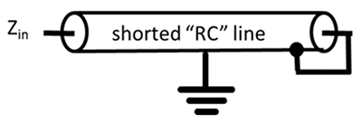
The very same physics as described by [2] is embodied in the 1D RC transmission line, as I’ve described in [3, 4], whereby electrical quantities like V are analogous to T, I to power P, specific heat Cp to capacitance C, and thermal conductivity k to resistance R. Figure 2 is from [3, 4], where a transmission line is shown shorted at its far end, simulating a perfect heat sink. The Wunsch-Bell (W‑B) treatment of [2] is for an infinitely long line, or for a terminated line at short time, i.e., heat diffusion length that is very short compared to its electrical length.
Make no mistake; the RC transmission line being analogous to heat flow and vice versa goes all the way back to the 19th century, even before J.C. Maxwell’s 1865 electromagnetics breakthrough. Early telegraph lines were thought to behave in accordance with heat flow equations and, of course, they do if signals are slow and inductive effects can be overlooked—in heat flow, there is no analogous magnetic effect. In the late 19th century, this was the source of much disbelief and consternation among telegraphy engineers even at the highest level, as described in accounts of the contributions of Oliver Heaviside [5].
By the early 20th century, things had settled down, and transmission lines were seen to be all of a piece, with or without inductance. Expressions for, say, Zin of Figure 2 in the frequency and time domains were well accepted, with the understanding that Fourier/Laplace transforms and their inverses, plus the convolution theorem, help one to go back and forth between time and frequency domains.
The beginning student in electrical engineering may know little more about electricity than Ohm’s Law, V=IR, but soon finds, in introductory courses, that it becomes generalized, with complex numbers applying to impedances (beginning with inductors and capacitors) as well as to voltage and current signals. Our student quickly learns that the generalized V=IZ, with multiplication, applies only to the complex frequency domain, as in V(s)=I(s)Z(s), where s=s+jw. Conversion to time domain requires transforms and multiplication is replaced by convolution, as in V(t)=I(t)⊗Z(t) or V(t)=I(t)*Z(t), the notorious “sliding integral.”
At this point, many students wish for a future full of simple resistors, able to migrate without difficulty between time and frequency domains. The mathematical treatment of an impedance with a time-dependent response can be challenging—also, there is well-meaning learning material on the internet with careless or incorrect statements about impedance and time/frequency domain. No, you will not see a reference to such misinformation here, given the influence of references on search engines. Just beware.
Now we are well-equipped to find surface temperature waveforms given the power input into a structure represented by Figure 2, where Zin(s)= Z0(s) tanh(τs), τ the line length, infinite for W-B conditions. Thus, the tanh factor becomes one for W-B, in which case we are left with Z0(s). Transmission line characteristic impedance for the general RLGC line is well known to be:
![]() (1),
(1),
But for our RC line, G=L=0, and therefore:
![]() (2)
(2)
Thus, if the power input P(s) (resembling current I(s)) is a step function going as 1/s, finding the temperature (resembling voltage) waveform T(t) from T(s) means looking up the inverse Laplace Transform of s-3/2, going as t1/2. Thus, for a critical temperature Tc, the time to failure for a given input power P0 goes as t-1/2, the W-B result.
This simple and lucid way of reaching the W-B result through Laplace Transforms was overlooked by the authors of [2] although the attractiveness of Laplace methods for heat flow problems was documented in renowned texts much earlier, for example in Carslaw and Jaeger [6]. Even [6] can be annoying in its reluctance to use the Laplace method to show how simple problems, such as the above, become even simpler, preferring to reserve the Laplace method for very difficult heat flow cases. That choice may have made more sense in 1959 and earlier, when [6] was published in a world where we had fewer engineers versed in network theory who needed to know about heat flow. But once the Laplace “infrastructure” is available in one’s mind from other studies, it is an attractive way to treat these heat problems.
If the heat slab is infinitely deep and the line in Figure 2 is infinitely long, the W-B result of a t1/2 waveform means that T(t) increases without limit if constant power P0 is continuously applied. But a resistive termination or short, as shown in Figure 2, means that a steady state is reached at some time scale, and the structure behaves like a constant thermal resistance (more precisely, conductance per unit area) to ground. This means that as the P0(t) pulse lengthens, the time to failure flattens out, as in Figure 3.
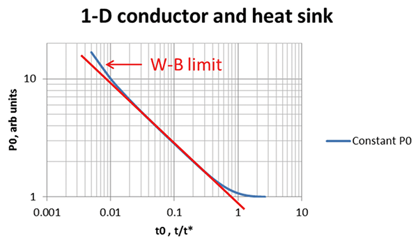
The complete curve is called the Dwyer curve, after a lead author who described it over 30 years ago [7, 8]. The transition from W-B region to a flat curve has been described in various ways, but my approach in 2016 [3, 4] was to invert the complete Zin(s) function in tanh form, as above, into the time domain. The result is a smooth function (a centuries-old theta function due to Jacobi) with the expected asymptotic limits. This is a fine “discovery” if your situation really is close to a 1D heat slab with a heat sink underneath—not always the case. Still, if you need a smooth curve and a single time constant t* to characterize the depth of the semiconductor and flattening of the curve, this can work, as shown in [3, 4].
I’ll close this article by summarizing some work done on integrated circuit metal heating during ESD, considering defined pulsed currents, self-heating of the metal due to positive temperature coefficient of resistance (TCR, or tempco), with attendant feedback effects on the power function P0(s)⇔P0(t) and then the final waveform T(t).
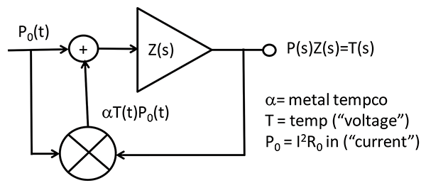
Publications appeared at IRPS in 2013 and 2016 [9, 10], in which the heart of the analysis was the metal self-heating feedback situation as shown in Figure 4, from [10]. The objective was to find an efficient way to arrive at ESD design rules for metal cross-section given that standardized waveforms I(t) for the human body model (HBM) and charged device model (CDM) would be applied to the IC pins. As the power input is TCR and feedback-dependent, we had to arrive at self-consistent power and temperature functions.
These studies benefited from finite element modeling (FEM) of the temperature response to a heating step applied to a length of metal, embedded in a “typical” array of other metal lines, oxides, dummies, etc., in accordance with design rules. With that data, we have a step response, and thus an impulse response, to heat input that gives us Z(t) and, implicitly Z(s). Convolution in the time domain is done (with plugin Excel tools) to reach a self-consistent output temperature waveform T(t)—fortunately, convergence is fast.
The studies are aimed at formulating ESD design rules for IC metal at various metal levels in the on-chip stack, so we input the anticipated current waveforms for HBM and CDM and find conditions for staying below a critical peak temperature for the ESD test goal. FEM electrothermal sims are capable of incorporating the test current waveform and metal properties to give a T(t) waveform as well, but once we get going with the feedback model, FEM can be reserved for cross-checks and fine-tuning of Z(t) for a given metal layer.
Process corners and variations can all be examined quickly by the feedback model, which became further simplified (as discussed in [10]) by certain regularities found in Tmax as produced by Jmax for HBM and CDM waveforms. The result was a tremendous leveraging of the FEM data, and much increased confidence that aggressive ESD design rules for metal would result in low peak temperatures, even at process corners.
As shown, Figure 4 has a peculiar mix of time and frequency domain expressions although, as above, all calculations are time domain. I could have expressed the thermal Ohm’s Law output as P(t)*Z(t)=T(t)—better use * as the convolution operator here, given our multiplier node in the feedback circuit. But I wanted to distinguish that concept, and operation, from the actual time domain multiplication that happens due to the metal tempco.
There is more in the references [9, 10] to clarify this, but the whole scheme requires some careful thinking—
be glad we have FEM sims for cross-checking! Figure 4 and the work surrounding it in [9, 10] is the trickiest example I’ve encountered of thermal Ohm’s Law in the time and frequency domains.
References
- J.S. Smith, “Electrical Overstress Failure Analysis in Microcircuits,” 1978 International Reliability Physics Symposium Proceedings, pp. 41-58.
- D. C. Wunsch and R. R. Bell, “Determination of Threshold Failure Levels of Semiconductor Diodes and Transistors Due to Pulse Voltages,” IEEE Trans. Nucl. Sci., NS-15, pp. 244-259, 1968.
- T.J. Maloney, “Unified Model of 1-D Pulsed Heating, Combining Wunsch-Bell with the Dwyer Curve,” 2016 EOS/ESD Symposium, paper 7A.2, Sept. 2016.
- Appendix B, White Paper 4 (free to the public)
- Paul J. Nahin, Oliver Heaviside: The Life, Work, and Times of an Electrical Genius of the Victorian Age, Baltimore and London: The Johns Hopkins University Press, 1988 and 2002.
- H. S. Carslaw and J. C. Jaeger, Conduction of Heat in Solids, 2nd edition. Oxford, UK: Oxford University Press, 1959.
- V. M. Dwyer, A. J. Franklin, and D. S. Campbell, “Thermal Failure in Semiconductor Devices,” Solid State Electronics, vol. 33. pp. 553-560, 1990.
- V. M. Dwyer, A. J. Franklin, and D. S. Campbell, “Electrostatic Discharge Thermal Failure in Semiconductor Devices,” IEEE Trans. Elec. Dev., vol. 37, no. 11, pp. 2381-87, Nov. 1990.
- T. J. Maloney, L. Jiang, S. S. Poon, K. B. Kolluru, and AKM Ahsan, “Achieving Electrothermal Stability in Interconnect Metal During ESD Pulses,” 2013 International Reliability Physics Symposium Proceedings, paper EL-1.
- T.J. Maloney, “Modeling Feedback Effects in Metal Under ESD Stress,” 2016 International Reliability Physics Symposium Proceedings, Paper 6A.4 (Pasadena, CA, April 18-21, 2016).