Introduction
Charged Device Model (CDM) testing is at a crossroads. For the last decade, the Industry Council on ESD Target Levels has recommended that CDM levels of 250 V, as measured with the field-induced CDM test method JS-002[1], are sufficient for high yield manufacture in facilities with basic ESD control [2]. Until recently, integrated circuit manufacturers have routinely provided products meeting the 250 V level and above. This is changing. High-speed interfaces such as 100 Gb/s and above SerDes can no longer meet both the required speed and deliver 250 V CDM levels. ESD protection circuits for 250 V CDM have too much loading capacitance for such high-speed applications. For this reason, the Industry Council has modified its CDM recommendations in the latest update of its CDM white paper [3]. Most devices should continue to meet the 250 V CDM target level but acknowledge that ultra-high-speed pins will no longer be able to reach that level. The Council did not, however, recommend a target of 125 V CDM, the next lowest classification level in JS-002. The Council advised that CDM levels be as close to 250 V levels as practical while meeting performance goals. Dropping CDM levels all the way to 125 V could have severe implications for device yield in manufacture and assembly. This requires a CDM test method providing reliable measurements in the 125 V to 250 V range with an accuracy, repeatability, and reproducibility on the order of 20 V. This cannot be met by JS-002 below 250 V. [4]
Background
Most ESD experts consider CDM testing to be the most critical ESD qualification test for modern integrated circuits. CDM testing emulates the fast discharge that a charged integrated circuit will experience if it makes metallic contact to a grounded surface. This is just the kind of ESD stress expected in a modern printed circuit production line. Printed circuit boards automatically and rapidly move from place to place while high-speed robotic arms grab components from trays or off reels and place them on the circuit board. Speed is of the essence, resulting in a multitude of chances for electrostatic charging and discharging. Factory ESD experts work hard to minimize device charging and control discharges, but all components must have some ability to survive the discharges they may be exposed to. The ESD control engineers need to know the charged device ESD robustness of all components passing through their manufacturing line. CDM measurements provide that knowledge.
Field-Induced CDM Testing
Field-induced CDM is the most widely used CDM test method today. Figure 1 shows a diagram of the CDM test fixture as well as a circuit diagram overlay for field-induced CDM testing according to JS-002[1]. In field-induced CDM an uncharged integrated circuit is placed on a thin insulator on top of a field plate. The field plate is then brought to a high potential. Capacitive coupling elevates the potential of the integrated circuit to a voltage close to that of the field plate. The integrated circuit is then rapidly grounded by touching a pin on the circuit with a pogo pin tied to ground with a 1-ohm resistor. The grounding of the integrated circuit often creates a sub ns pulse of up to several amps, replicating the type of stress a circuit could see during manufacture. The test is repeated with both positive and negative field plate voltages for all pins on the circuit. After stressing all pins, positive and negative, the device still needs to meet all datasheet and functional specifications.
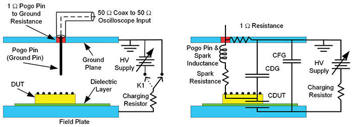
Field-induced CDM has worked well for the industry for many years, but the test results become erratic below 250 V due to the erratic nature of air discharges at low voltages. [4] As stated above, there is an urgent need for an improved test method, and it is generally agreed that the air discharge must be eliminated. Fortunately, there are several candidates.
Low Voltage CDM Options
Four possibilities will be discussed, two based on direct charging and two based on transmission line pulse (TLP) testing techniques. In each method, the air discharge of field-induced CDM is replaced by discharge in a relay.
JEITA CDM Test
There is already one CDM test standard that does not have issues at low voltage levels, the Japan Electronics and Information Technology Industries Association (JEITA) standard JEITA ED-4701/302A test method 305. [5] This test method, shown in Figure 2, has not been very popular outside of Japan. The JEITA method uses direct charging as opposed to field-induced charging. The electrode touches the pin to be tested, and then the potential is raised to an elevated potential through high-value resistors. A switch then grounds the pin being tested. The use of a switch to initiate discharge removes most of the issues of low voltage testing.
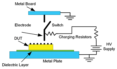
While this method gives useful information, there are several issues with the JEITA CDM test method. The relay geometry will add inductance to the discharge path, slowing the CDM discharge. The method for performing waveform verification inserts a current probe and an additional length of wire, both of which are not present during device testing. This raises the issue of how well the verification waveform matches the waveform experienced by devices being tested. The JEITA test method also calls for a 2 GHz oscilloscope rather than the 6 GHz oscilloscope required by JS-002. This can hide waveform artifacts that could affect test results. As written, the JEITA standard does not include a method for measuring device waveforms during device stress, preventing waveform measurement during device stress. Fortunately, at least one equipment manufacturer includes a 1-ohm resistor between the relay and the ground board, similar to JS-002, allowing waveform verification during device stress. The test method’s low voltage performance does make it an attractive alternative to field-induced methods at low voltage.
Contact CDM
The contact CDM method [6][7] is shown in Figure 3. Contact CDM uses a test head very similar to that used in JS-002, except that the 1-ohm resistor is removed. The coaxial cable, which in JS-002 connects directly to an oscilloscope through an attenuator, instead connects to a 50-ohm switch. The switch leads to either a resistor and high voltage supply or to an attenuator and oscilloscope. During testing, the device is charged slowly to a high voltage, and the switch is then moved to the oscilloscope triggering a discharge. The device’s stress current is determined by subtracting a pulse measured without the device from a measured pulse with the device connected.
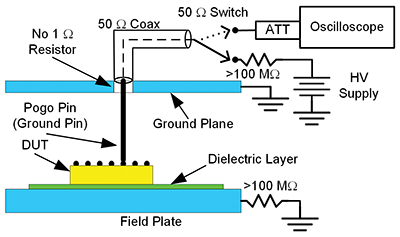
Contact CDM produces a very repeatable stress to the device being tested. The 50-ohm characteristics of the relay minimize degradation of the measured waveform. An issue with contact CDM is that the impedance that the device sees is 50 ohms, not the much lower impedance of an air discharge.
Capacitively Coupled TLP
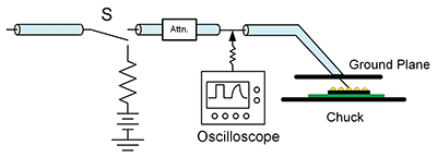
Capacitively coupled TLP (CC-TLP) was introduced almost 20 years ago [8] but has been getting increased attention as a potential extension of CDM testing to lower voltage [9]. In CC-TLP, illustrated in Figure 4 Capacitively coupled TLP. A very fast TLP (vf-TLP) system is used to stress an integrated circuit using a special CC-TLP probe. The probe consists of a ground plane connected to the shield of the coax pulse delivery cable. The center conductor of the cable is connected to a probe that extends through a hole in the ground plane and can touch a pin on the device under test (DUT). The DUT is placed on a thin insulator on top of a chuck. To stress the device, a short TLP pulse is delivered to the probe touching the DUT. The capacitance between the DUT and the ground plane provides the return path from the probe back to the outer shield of the vf-TLP’s pulse delivery cable. This system can deliver pulses with similar current levels and time durations as a CDM stress. Since the pulse is started with the closing of a relay, the delivered pulses are very reproducible, even at low voltages. Another advantage of CC-TLP is that testing can be done either at wafer level or on a packaged device.
Low Impedance Contact CDM
The final candidate for low voltage CDM testing, and one of the most promising, is low impedance contact CDM (LICCDM) [10][11], shown in Figure 5. This system uses a modified version of the JS-002 test head. In this system, a short vf-TLP pulse is passed through a rise time filter which leads to the test head and the device pin being tested. The rise time filter matches the pulse rise time characteristics of JS-002. The capacitor and 50-ohm resistor slow the falling edge of the pulse so that the leading edge dominates the capacitively coupled stress to the device being tested. Also connected to the device pin is a second coaxial cable leading to an attenuator and oscilloscope as well as a 50-ohm connection to ground. Stress pulses are measured by the oscilloscope. Pulses are performed at the same stress levels with and without contact to the device being tested. The stress current to the device can be calculated from the with and without contact pulses and the known 50-ohm impedances of the two coaxial cables and the 50-ohm resistor to ground.
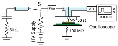
The presence of the two 50-ohm coaxial cables and the 50-ohm resistance to ground means that the device pin sees three 50-ohm impedances in parallel or an impedance of 16.7 ohms. This is very close to the resistance of an air discharge. This implies that the stress to the device should closely resemble a field-induced CDM stress if the peak heights and durations are similar.
What Needs to Be Done?
In the short term, any of these four methods can provide information for charged device robustness at low voltages, but none of them is universally accepted. The question is how their stress levels compare with the current JS-002 test method. Correlation with JS-002 is important for ESD control engineers so that they understand the level of ESD sensitivity they need to prepare for. The joint JEDEC/ESDA (Electrostatic Discharge Association) CDM Working Group is currently doing extensive comparisons between the JS-002 and the other CDM options, with particular emphasis on LICCDM and CC-TLP.
References
- ANSI/ESDA/JEDEC JS-002 – 2019, “Joint Standard For Electrostatic Discharge Sensitivity Testing Charged Device Model (CDM) – Device Level,” joint standard of JEDEC and Electrostatic Discharge Association.
- JEP157, “Recommended ESD-CDM Target Levels,” JEDEC publication 2009.
- JEP157A, “Recommended ESD-CDM Target Levels,” JEDEC publication (pending March 2022).
- N. Jack, B. Carn, and Josh Morris, “Toward Standardization of Low Impedance Contact CDM,” EOS/ESD Symposium Proceedings, 2019.
- JEITA ED-4701/302 “Test method 305C Charged device model electrostatic discharge (CDM/ESD),” Japan Electronics and Information Technology Industries Association.”
- R. Given, M. Hernandez, and T Meuse, “CDM2 – A New CDM Test Method for Improved Test Repeatability and Reproducibility,” EOS/ESD Symposium Proceedings, 2010.
- ESD TR5.3.1-01-18, “For Electrostatic Discharge Sensitivity Testing Contact Charged Device Model (CCDM) vs. Field Induced CDM (FICDM) a Case Study,” Electrostatic Discharge Association, 2018.
- H. Wolf, H. Gieser, W. Stadler, and W. Wilkening, “Capacitively coupled transmission line pulsing CC-TLP – A traceable and reproducible stress method in the CDM-domain,” EOS/ESD Symposium Proceedings, 2003.
- J. Weber, K. Kaschani, H. Gieser, H. Wolf, L. Maurer, N. Famulok, R. Moser, K. Rajagopal, M. Sellmayer, A. Sharma, and H. Tamm, “Correlation study of different CDM testers and CC-TLP,” EOS/ESD Symposium, 2017.
- N. Jack and T. Maloney, “Low Impedance Contact CDM,” EOS/ESD Proceedings, 2015.
- ANSI/ESD SP5.3.3-2018, “For Electrostatic Discharge Sensitivity Testing, Charged Device Model (CDM) Testing – Component Level, Low-Impedance Contact CDM as an Alternative CDEM Characterization Method,” Electrostatic Discharge Association, 2018.
