
Inductance is one of the most misunderstood and misused concepts in electrical engineering. While in school, we learn about inductors, small components we can hold in our hands and lumped elements we can put in a SPICE circuit, but we seldom learn about inductance.
We also learned that “inductors” have a property that causes their impedance to increase as frequency increases (Equation 1) and that, when combined with capacitors, they produce resonant circuits. While inductors certainly have inductance (when used in a circuit), we do not need a physical inductor to have inductance!
![]() (1)
(1)
Where:
XL is the inductive impedance
f is the frequency
L is the inductance
Why Is This Important?
We are constantly exposed to products and components which claim to have low inductance. This is one of the main causes of the misunderstandings surrounding inductance.
The fundamental fact is that the only time we have inductance is when there is a loop of current. Without the current loop, we cannot have inductance. Of course, as soon as there is current, the current must return to its source, so there will always be a current loop whenever there is current. This is a fundamental fact of physics. The goal of this article is to try to dispel some of the misconceptions surrounding inductance and to encourage engineers to think more clearly about these physics.
Definition of Inductance
The definition of inductance comes from Faraday’s Law (Equation 2). If we dissect this equation and relate it to Figure 1, we see that both sides of the equation require a loop. The left-hand side is the integral (or simply the summation) around a closed loop of the electric field multiplied by the length (which is simply the voltage). The voltage around the loop is the same as the voltage across a small gap, as shown in Figure 1. The point is that a loop is required creating the loop inductance.

Figure 1: Simplified geometry for Faraday’s Law
![]() (2)
(2)
When we look carefully at the right-hand side of Faraday’s Law, we see that there is a double integral (area of a surface) where the amount of time-varying magnetic flux density within the surface area is summed. Since there is a surface, there must be a defined perimeter, again forming a loop.
The standard unit of inductance is the henry. It is a derived unit that relates the amount of negative voltage created by a time-varying current. If the rate of change of the current is 1 ampere/second, then one henry will induce a voltage across the gap (with a magnitude of negative one volt) to resist the change in current.
If the time-varying magnetic field within the surface area is not changing with position (an electrically small loop, for example), then Faraday’s Law reduces to Equation 3.
![]() (3)
(3)
If we now induce a time-varying current in this loop, there will be a time-varying magnetic flux within the loop. Equation 3 shows us that there will be a negative voltage induced in the loop, effectively impeding the initial flow of current. Clearly, as the size of the loop area becomes larger, the amount of negative voltage (inductive impedance) will increase. The loop area is the primary physical effect that controls the amount of inductance a current will experience.
It is common for someone to expect the inductance of a circuit will be reduced by increasing the conductor size. This will be examined a little later, but it is worth the time to look at a simple formula for finding the inductance of a simple isolated loop. Equation 4 allows us to calculate the inductance of a wire loop [1].
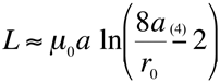 (4)
(4)
Where:
L = loop inductance
a = loop radius
r0 = wire radius
The size of the loop is determined by a, the radius of the loop. This radius is both outside the natural log function and inside the function. The radius of the wire, r0, is only within the log function, and so the inductance varies much more slowly with the radius of the wire. Figure 2 shows the relative change in total loop inductance as either the loop radius or the wire radius changes. It is clear that the loop area has a much more significant impact on loop inductance. (The relative impact of the wire size was so small compared to the loop area that a log scale was required to see the effect of wire radius change!)

Figure 2: Relative impact on loop inductance from Equation 3
The bottom line is that a loop must be defined before the term ‘inductance’ has any meaning. A simple, straight wire, a braided ground strap, and a surface-mounted capacitor do NOT have inductance by themselves! We could discuss the partial inductance of those items, but until the loop is defined, the inductance is not defined. (Partial inductance will be briefly explained in a later section.)
When a vendor discusses the inductance of a braided ground strap, how the inductance is determined should be understood so that the user can determine if the braided strap will or will not perform in a similar fashion in his or her application. Similarly, a surface-mounted capacitor often has a specification for an equivalent series inductance (ESL). How is this possible without defining the loop where the current will flow? Again, we need to understand the measurement process. The vendor simply places the capacitor over a very thin insulator with a ground plane beneath it. A voltage is applied between the capacitor’s port #1 and ground-reference, the current flows through the capacitor and returns directly below in the ground plane, forming as small a loop as possible. Of course, when the capacitor is used in a real-world printed circuit board and connects to internal PCB layers, the amount of actual inductance is much greater than in the ideal ESL.
Decoupling Capacitor Connection Inductance
As mentioned in the above section, the actual inductance of a decoupling capacitor mounted on a PCB is much higher than the vendor’s reported ESL. The connection inductance depends on the distance between the vias and the distance from the top (or bottom) mounting location to the planes that are to be decoupled. (Connection inductance is considered to be ‘above the planes’ only and does not consider the separation between the power and ground planes, nor the distance from the capacitor to the observation point.) Figure 3 shows a side view of a typical decoupling capacitor mounting on a PCB.
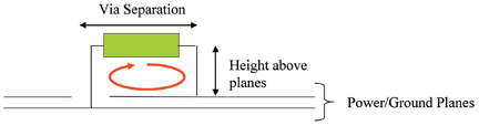
Figure 3: Typical surface-mounted decoupling capacitor loop inductance
It is obvious that if the vias are placed close together and the planes to be decoupled are near the top of the PCB (when the capacitor is mounted on the top of the PCB), the connection inductance, represented by the loop, will be minimized. However, there are limits to how close the vias can be placed due to manufacturing issues. There are also limits to how close to the top surface the power/ground-reference planes can be located. So it is important to understand how the mounting will affect the performance of the capacitor and the connection inductance [2].
Connection inductance alone does not tell the complete story. The inductance associated with the spacing between the power/ground-plane pair, as well as any inductance associated with the distance between the IC and the decoupling capacitor, is not included in the connection inductance calculations.
Figures 4 and 5 show common mounting configurations for capacitors of size 0603 and 0402, respectively, for typical manufacturing limits. Table 1 shows some calculated connection inductances (without ESL) for 0805, 0603, and 0402 size SMT capacitors for different depths to the power/ground-reference plane pairs [3-4]. (See references for details on the formula used for this calculation.)

Figure 4: Typical minimum 0603 capacitor mounting dimensions
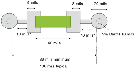
Figure 5: Typical minimum 0402 capacitor mounting dimensions

Table 1: Connection inductance for typical capacitor configurations
These values are calculated with the example of 7-8 mils from capacitor-to-mounting-pad-edge, 20 mils from capacitor-mounting-pad-edge-to-via-pad, via pad diameter of 20 mils, via barrel size of 10 mils, and trace width equal to 20 mils. The absolute minimum distance from via pad to capacitor mounting pad edge is reported to be 10 mils, but typically 20 mils is used to be safe.
The distance between the via pad and the capacitor mounting pad was kept to a small value in the above calculations. If this distance is increased slightly to 50 mils, the connection inductance increases to the values in Table 2.
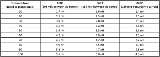
Table 2: Connection inductance for typical capacitor configurations with 50 mils from capacitor pad to via pad
The connection inductance plays a much greater role in the performance of decoupling capacitors than the typical ESL of these components. Connection inductance values of 1 to 3 nanohenries are typical with the most common surface-mount capacitor sizes and manufacturing technologies. Using the tables, engineers can decide if a decoupling capacitor is better placed on the top or bottom surface of the PCB in order to provide charge to the power/ground-reference plane pairs.
Mutual Inductance
Mutual inductance is a measure of the current induced in a second loop, due to the flux from the first loop (Figure 6). As described above, a time-varying current in the first loop will create time-varying magnetic flux. If a second loop is close to the first loop, a significant portion of this magnetic field flux will penetrate the second loop, inducing a time-varying current in the second loop.
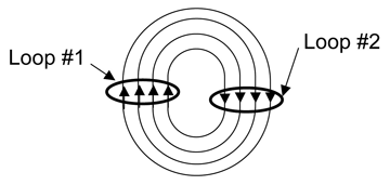
Figure 6: Mutual inductance from current in one loop creating flux in second loop
Figure 6 shows the two loops in a co-planar orientation. If they are oriented perpendicularly to each other, then the lines of flux from Loop 1 will not penetrate Loop 2, and there will be no mutual inductance. (This is approximate. There would be a small amount of flux lines within the conductors, creating a small amount of mutual inductance.) If one of the loops is made much smaller, then the amount of flux is reduced, again reducing the mutual inductance. And finally, as the loops are moved further apart, the magnetic flux penetrating the second loop decreases rapidly, which also reduces mutual inductance.
Partial Inductance
The definition of inductance requires a current flowing in a loop. Without a complete loop, there cannot be inductance. Practical considerations, however, lead us to discuss the inductance of a part of the overall current loop, such as the inductance of a capacitor. This idea of discussing the inductance of only a portion of the overall loop is called partial inductance [4]. Partial inductances can be combined to find the overall inductance. For the simple case of a rectangular loop of wire where sides 1 and 3 are parallel to each other and so are sides 2 and 4 (see Figure 7), Equation 5 can be used to calculate the total inductance from the partial inductances.
![]() (5)
(5)
Figure 7 shows this distributed inductance concept and relates back to Equation 5. In each portion of the loop we assign a partial inductance value as well as partial mutual inductance between all parts of the loop. (In this case, we only show the partial mutual inductance of the parallel sections, since perfectly perpendicular conductors will not have any mutual inductance.) Though the conductors may have different sizes, it is not a problem to calculate the partial inductance values. Naturally, if the current follows a more complex path, additional partial inductances and partial mutual inductances will be needed.
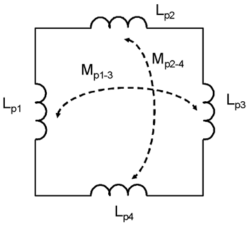
Figure 7: Partial inductance components of simple rectangular loop
The concept of partial inductance is especially useful when the physical geometry is complex and it is difficult to assign the loop inductance to any one location around the loop. For example, Figure 8 shows current flow from the power plane in a PCB through the output driver of an IC, through a trace to the IC load, and finally through the ground-reference plane back to the power supply source. Since there is a closed loop of current, there is an inductance associated with that current path … but where could we place the loop inductance in this circuit? First of all, since the various conductors have different sizes, it would be impossible to find a formula to find the loop inductance. However, since we know this inductance exists (even if we cannot calculate it easily), where would we place the inductance? If we choose location ‘A’, then we ignore any voltage drop in the other conductors due to inductive impedance. The same is true for the other locations (B, C, and D). The inductance is actually a distributed quantity and must be considered to be throughout the loop. The concept of partial inductance allows us to do this.

Figure 8: Current path for data through IC gates
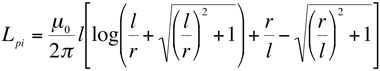
The partial inductance for a length of wire is given by (6), and the partial mutual inductance between a pair of parallel wires is given in (7).
 (6)
(6)
 (7)
(7)
Where:
l = length of wire
r = radius of wire
d = distance between parallel wires
Figure 9 shows the partial mutual inductance for two parallel 10 cm long wires. Note that when the wires are close together, the partial mutual inductance is very high. Referring back to (5), we see that when the partial mutual inductance is high, the total inductance is low (because it is subtracted). When the wires are close, the loop area would be smaller, resulting in a lower inductance, as expected. Calculations for more complex geometries can be found in [5].
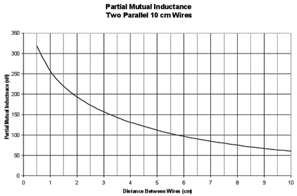
Figure 9: Example of partial mutual inductance of a pair of parallel wires
Summary
The basic principle that inductance requires current to flow in a loop is an important concept to understand. This is not unreasonable since current must flow in a loop. The size of the current loop determines the amount of inductance.
Inductance is a basic building block in electronic circuits. That is, as soon as metal conductors are used and current flows through them, inductance exists. This inductance becomes the limiting factor in all high-frequency circuits. When capacitors are used as filter elements, the natural inductance associated with the current flowing though the capacitor limits the frequency range where the capacitor is an effective filter component.
Partial inductance is a useful concept, since with partial inductances one can discuss the contribution of a single part of the loop to the total inductance. An example is the via connecting between different layers on the PC board, the metal stand-off post between the PC board and the chassis, and traces on the PC board connecting filter components. Each of these metal structures can be analyzed to find their partial inductances, and the results can then be combined to find the total inductance.
This has been a very brief introduction to inductance. A much more complete study of this subject is available in the references.
![]()
References
- F.W. Grover, Inductance Calculations, Dover Publications, NY, 1946.
- James L. Knighten, Bruce Archambeault, Jun Fan, Samuel Connor, and James L. Drewniak, “PDN Design Strategies: II. Ceramic SMT Decoupling Capacitors – Does Location Matter?,” IEEE EMC Society Newsletter, Issue No. x, Winter 2006, pp. 56-67. (www.emcs.org)
- Jun Fan, Wei Cui, James L. Drewniak, Thomas Van Doren, and James L. Knighten, “Estimating the Noise Mitigating Effect of Local Decoupling in Printed Circuit Boards,” IEEE Trans. on Advanced Packaging, Vol. 25, No. 2, May 2002, pp. 154-165.
- A.E. Ruehli, “Inductance Calculations in a Complex Integrated Circuit Environment,” IBM J. Research and Development, 16, pp 470-481, 1972.
- C. Paul, Inductance: Loop and Partial, Wiley, 2009.
Dr. Bruce Archambeault and Sam Connor bring their experience at IBM to the issue of inductance and EMC, while Mark Steffka shares his expertise developed at General Motors.
 |
Dr. Bruce Archambeault is an IBM Distinguished Engineer at IBM in Research Triangle Park, NC and an IEEE Fellow. He received his B.S.E.E degree from the University of New Hampshire in 1977 and his M.S.E.E degree from Northeastern University in 1981. He received his Ph. D. from the University of New Hampshire in 1997. His doctoral research was in the area of computational electromagnetics applied to real-world EMC problems. He is the author of the book “PCB Design for Real-World EMI Control” and the lead author of the book titled “EMI/EMC Computational Modeling Handbook”. |
 |
Sam Connor is a Senior Technical Staff Member at IBM and is responsible for the development of EMC and SI analysis tools/applications. Mr. Connor’s current work activities and research interests also include electromagnetic modeling and simulation in support of power distribution and link path design for printed circuit boards. He has co-authored more than 20 papers in computational electromagnetics, mostly applied to decoupling and high-speed signaling issues in PCB designs. He is a Senior Member of the IEEE and is currently the Chair for the TC-9 subcommittee of the IEEE EMC Society. |
 |
Mark Steffka, B.S.E., M.S. is a Lecturer (at the University of Michigan – Dearborn), an Adjunct Professor (at the University of Detroit – Mercy) and an automotive company Electromagnetic Compatibility (EMC) Technical Specialist. His university experience includes teaching undergraduate, graduate, and professional development courses on EMC, antennas, and electronic communications. His extensive industry background consists of over 30 years’ experience with military and aerospace communications, industrial electronics, and automotive systems. Mr. Steffka is the author and/or co-author of numerous technical papers and publications on EMC presented at various Institute of Electrical and Electronics Engineers (IEEE) and Society of Automotive Engineers (SAE) conferences. He has also written about and has been an invited conference speaker on topics related to effective methods in university engineering education. He is an IEEE member, has served as a technical session chair for SAE and IEEE conferences and has served as an IEEE EMC Society Distinguished Lecturer. He holds a radio communications license issued by the United States’ Federal Communication Commission (FCC) and holds the call sign WW8MS. |