In Part 1 of this series, we introduced embedded detection technology, which augments basic protection against ESD events, and explored the opportunities for embedded ESD detection solutions.
Protection sets the fundamental thresholds for a device’s robustness. In contrast, detection broadens the device’s awareness around these limits, helping it identify potential issues such as data corruption, immediate damage, or the cumulative effects of ESD within these thresholds. Armed with this, the designer has an opportunity to design in recovery functionality rather than just accept a mysterious malfunction.
Here, in Part 2, we shift our focus to the practical aspects of implementing embedded ESD detection. We’ll provide a step-by-step guide, discuss validation and testing methodologies, present case studies, and delve into future trends and innovations in the field.
Preparing for Embedded ESD Detection
As technology process nodes advance, the susceptibility to physical damage from a given ESD event increases, but on-chip HBM and CDM protection is also advancing to protect these delicate nodes. However, these advanced on-chip ESD protection devices are typically designed to protect the chip when powered off, during PCBA assembly and only under factory ESD controls. As these protection circuits clamp harder and faster, they can even prevent the off-chip discrete protection from triggering, making the whole system counter-intuitively less robust.1 Protection circuits that are designed to clamp VDD to VSS can cause extensive data corruption and state incoherence inside the running chip. This leaves device registers, oscillators, and logic in unpredictable and unknown states at worst and in a sudden and unexpected Power-on-Reset (POR) vector at best.
Balancing ESD Protection with ESD Detection
External system-level ESD protection devices are typically not (yet) super-conducting, and so there is some residual current sharing with the Device Under Protection (DUP) ASIC or SoC, etc.
This residual pulse is not necessarily shaped like the CDM or HBM standards the chip has been designed for, and typically, these protections are intended for activation during assembly when no power is applied. Complaining to the IC manufacturer that their chip does odd things when exposed to ESD brings to mind the old story of a man telling his doctor, “It hurts when I do this.” To which the doctor replied, “Then don’t do that.” The reality is there is no standard for validating chip-level functionality after an ESD strike, and so the system designer is left to manage it or, worse, to blame the susceptibilities on firmware. “Here be dragons,” they say.
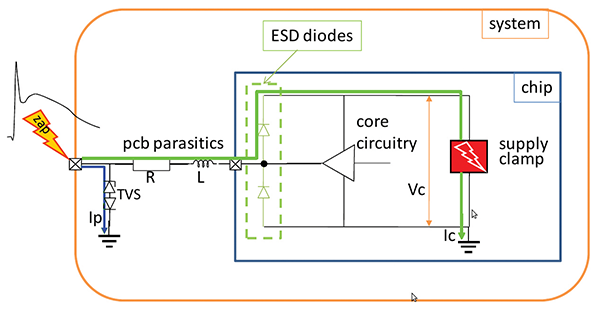
- Soft-Reset: When a system successfully survives an ESD zap, the HBM or CDM on-chip protection may trigger its on-board power supply clamps that short VDD to VSS to minimize voltages throughout the chip. (See Figure 1.) Once the pulse has dissipated, the power rails will return to their pre-zap levels and may trigger Power-on Reset (POR) circuits, resetting the system. If the firmware is aware that an ESD event has been detected just before POR has occurred, then the software can take additional remedial and recovery actions.2
- System Lockup: As with a soft reset, when the on-chip protection occurs, the logic state and coherency cannot be trusted. In fact, the MCU or Crystal Oscillator may run “off into the weeds” and require a hard power cycle, which may not be possible in mission-critical and medical devices. However, embedded ESD detection logic can recognize the event and “kick start” the device back to life. If the software is written in such a way that the user does not notice this disruption, then such an upset has been effectively eliminated from an IEC qualification failure list without board spins, etc.
- Data Corruption: Any software programmer assumes that when a value is written to a location, it will be there when it is read back. However, after an ESD event, memory and registers, program counters, and stacks can be altered slightly or obliterated. This can sometimes create a latent “soft error,” which might not manifest itself for days or operation. An ESD event detector can alert the program to recheck the system state and restore corrupted areas or at least throw an error alert.
- Latent Circuit Damage: Even a survivable strike may significantly degrade component lifetimes.3 A system that has weathered 10,000 pulses is not necessarily as healthy over time and temperature as a system that has never been struck.
- TVS Optimization: By recording and perhaps transmitting ESD event telemetry back to the manufacturer, system designers can fine-tune the protection levels, potentially reducing cost by optimizing for the actual ESD levels the products are seeing in the field.

Embedded Detector Technologies
The application of ESD detectors to characterize system-level pulses and enhance robustness is relatively new, but ESD detector types and functionality have been under development for years. Here are some early examples that bracket the simple-to-complex options for implementation in between.
Basic ESD Detector: Peak-Hold Circuit
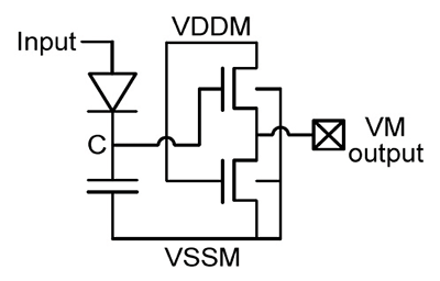
In 2011, Nathan Jack and Elyse Rosenbaum presented an on-die detector that could be probed at the wafer level.4 The node to be monitored is connected to a diode which dumps some of the incident ESD current into a capacitor which can be monitored by a buffer circuit. (See Figure 2.) This concept can be expanded to include multi-level detection and long-duration pulse memory.

Extreme ESD Detector: On‑chip Oscilloscope
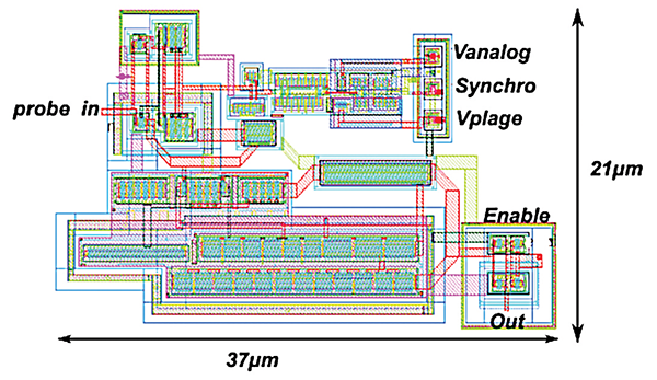
In 2013, Fabrice Caignet et al. demonstrated a 20 GHz on-chip oscilloscope detector circuit to reconstruct residual ESD voltages and analyze the pulse in more detail to help optimize the requirements for protection circuitry on a particular technology node going forward.5
As opposed to the simple level detector in [4], this circuit allows the reconstruction of the actual shape and spectral content of ESD pulses entering a chip.
These early examples of embedded detection have been complimented by the ongoing innovation and development in embedded on-chip ESD detection applications. As ICs continue to evolve and geometries shrink, these technologies may play an active role in preventing further technology nodes from becoming almost unusable due to ESD soft errors and upsets.

System-level ESD Detector: Discrete Test Module
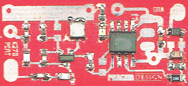
In some cases, a discrete detector may be adapted to an existing system with small PCBs or Flexible Attach Rework (FAR) modules (See Figure 4.) These “dead-bug” detectors can be used to record and transmit ESD events in a system to isolate entry/exit vectors and problematic nodes instead of adding probe cables which can alter the nature of the ESD pulse paths. Obviously, if the ESD detection capability is already integrated into the system, then gathering such data is faster, more reliable, and more convenient.

Conclusion
In Part 1 of this article series, we explored the critical need for embedded ESD detection in the context of advanced semiconductor nodes. The vulnerabilities of advanced ICs to ESD damage have necessitated the development of innovative solutions, such as embedded detection technology, to augment protection schemes. Embedded detection’s real-time monitoring and response capabilities offer a new level of overall robustness and reliability by expanding the visibility of ESD events and effects. In Part 2, we reviewed the basics of detection implementation in a system, along with a few examples to consider. In Part 3, we will outline practical aspects of implementing embedded on-chip or system-level ESD detection, providing engineers and designers with guidance on integrating these technologies into their semiconductor designs and ensuring the robustness of their electronic devices.
Endnotes
- W. Huang, J. Dunnihoo, and D. Pommerenke, “Effects of TVS integration on system level ESD robustness,” EOS/ESD Symposium, Reno, NV, 2010, pp. 1-6.
- White Paper 3 System Level ESD Part I: Common Misconceptions and Recommended Basic Approaches (v1.0 December 2010).
- I. Laasch, H-M. Ritter and A. Werner, “Latent damage due to multiple ESD discharges,” EOS/ESD Symposium, Anaheim, CA, 2009, pp. 1-6.
- N. Jack and E. Rosenbaum, “Voltage monitor circuit for ESD diagnosis,” EOS/ESD Symposium Proceedings, Anaheim, CA, 2011, pp. 1-9.
- F. Caignet, N. Nolhier, A. Wang, and N. Mauran, “20 GHz on-chip measurement of ESD waveform for system-level analysis,” EOS/ESD Symposium, Las Vegas, NV, 2013, pp. 1-9.
