When people are asked what is the most commonly used component in electrical or electronic circuits, the typical answers are “Well, of course everyone knows its resistors”, or “It must be capacitors”, and even sometimes “Nothing operates without transistors”. In fact, none of those answers are correct; the real answer is that conductors are the most common type of component.
Obviously, without conductors there would be no such thing as circuits. Even though conductors are the basic component of electrical circuits, there is surprisingly little consideration of the physics involved in conductors (outside of textbooks) and there seems to be even less emphasis on considering the characteristics of conductive structures (such as “chassis grounds”) when those conductors and conductive assemblies are used for the critical current return paths in a circuit. Perhaps this is because wires just don’t seem that exciting! Ironically, successful EMC engineering requires just such an understanding!
This article will refresh (or perhaps initiate) the reader’s knowledge and understanding of key aspects of conductors and conductive paths by looking at a number of topics, including:
- history of conductors.
- fundamentals of electrical energy propagation.
- types of wire conductors.
- models and characteristics of transmission lines.
- use of assemblies as conductive paths.
History of Conductors
Although wire made from conductive materials (such as iron or copper) has been in use for perhaps thousands of years, it was used as a mechanical component. It was not until a few hundreds of years ago (during the 1700s) that it was first used as a method to define a path for electrical current flow. Some of those first electrical uses were for protection of wooden structures in colonial America by the attachment of the conductive wire to iron “rods” placed on buildings to (hopefully!) provide a path for lightning strikes to be safely conducted to the earth instead of across the structure (which many times caused fires). The use of wire for this purpose (and the invention of the associated lightning rods) has been attributed to Benjamin Franklin.
During the early 19th century, as interest and worldwide fascination into “electrical flow” grew, Michael Faraday was among the first to perform empirical experiments to understand properties of conductors.
As the 1800s progressed, more uses for electricity were developed, including power distribution and communication (telegraph systems). As these systems became more complex, physically large, and capital intensive, there was an increasing desire to more fully understand these interconnection methods. As a result, Oliver Heaviside developed a number of important concepts and inventions during the 1880s, including transmission line theory and the “coaxial” style cable that we see today.
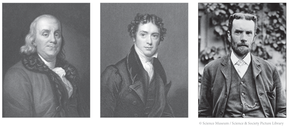
Figure 1: Pioneers in the use of conductors, Benjamin Franklin, Michael Faraday and Oliver Heaviside
What is the Purpose of a Conductor?
From the evolution of wires for lightning protection to power and signal distribution, and even to today, it can be seen that there is only one purpose of a conductor. That purpose is to provide an intended path for propagation of electromagnetic energy.
Therefore, a conductor is used to:
- provide power or signal(s) to where it’s needed.
- divert energy from where it’s NOT desired (such as in lightning grounds or surge suppression).
That intended path of electromagnetic energy is via “conduction”, as described by Professor Maxwell (in addition to his theory of “displacement current”, such as the current that “flows” through a capacitor).
In order to understand how energy is conducted from a source to a load, we start with the concept of the “idealized” energy transfer loop (as shown in Figure 2).

Figure 2: Schematic of basic or “ideal” energy transfer loop
“Idealized” Energy Transfer Loop
The figure shows the source of the power (or signal), represented by the “generator”. On the other side of the figure is the load (which can be represented by an impedance). The process of transferring the energy from the source to the load is via the conduction path, defined by the solid lines on the diagram). This transfer is typically explained as being similar to a current in water, in that there is a “current flow” along one conductor, while the other conductor functions as a “current return”. While this view is not incorrect, sometimes it is better to visualize the energy as an electromagnetic wave being guided from the source to the load.
Connection Path Impedance
Using the idealized energy transfer loop leads (unfortunately) to assumptions in system and circuit design that the conductive path is always characterized by a simple zero impedance connection. The problem is that in actual circuit construction, although conductive materials are used, these materials in reality have “non-zero” physical parameters (such as thickness, width, and material resistivity). Depending upon the physical size of the conductor(s), these actually need to be defined as having relevant volume or surface resistivity as shown in Figure 3. For volume resistivity, it is common to utilize a unit volume, such as a cube of equal dimensions in the X, Y, and Z
directions. For surface resistivity (when the thickness of the material is significantly less than the other dimensions) an X and Y dimension is used.

Figure 3: Defining the actual relevant volume and surface resistivity of a conductor
The way we typically establish conductive paths from sources to load is to use wires of various diameters (called “gauges”). Figure 4 shows various wire geometries and the common method for identifying the wire diameter. The resistance of wire is a function of both its material and physical dimension (typically diameter is expressed in “MIL”, which is equal to 0.001 inch).
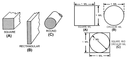
Figure 4: Various geometries of wire and methods for determining gauge
By using physical dimensions and material characteristics, it becomes a straightforward process to determine the resistance of any wire. This is shown below.
Calculation of the Resistance of Wires
- Resistance (R), is determined by ρ (rho), length (L), and cross sectional area (A).
- Example showing resistance for 1,000 feet of wire of 10,400 circular mils.

In this example, the 1,000-foot wire has a resistance of 1 ohm. It can be seen that if the length is doubled, the resistance will also double. This makes sense. An interesting observation can be made at this point, however, and that is if the cross-sectional area of the wire decreases (gets smaller), the resistance of the wire increases!
Wire Size (“Gauge”)
In order to provide consistency in wire selection and application, it is typically manufactured in sizes numbered according to the American Wire Gauge (AWG) tables. These tables show wire sizes from 0000 gauge (which is a 460.0 mil diameter for solid wire) to 40 gauge (3.1 mil diameter for solid wire). Of particular note is the fact that, according to these tables, a wire is a single rod or filament of drawn metal. Of course another type of wire is actually a number of solid wires bound together to function as a single wire. This more correctly is known as a stranded conductor or a cable. Table 1 shows DC parameters of typical cables of various AWG sizes. Figure 5 shows the difference between a single conductor wire and a stranded-conductor “wire”.
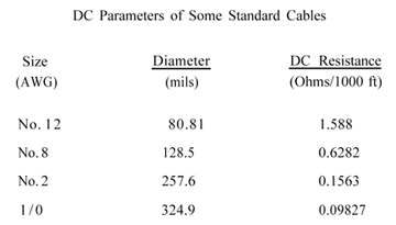
Table 1: Table showing DC resistance of different wires by gauge and diameter
Why do we have both solid and stranded “wires” (conductors)? It turns out that each has its own advantages that would make the selection of one or the other optimum for a particular application.
In the case of solid wires, they have the following attributes:
- cost-effective.
- high mechanical integrity (keeps form).
- smaller diameter for equivalent “gauge”.
Stranded wires, on the other hand would be used when the following characteristics are desired:
- flexibility.
- reduced “noise” (due to lower inductance compared with a similar length of solid wire).
- redundancy (some broken solid wires will not affect functionality).
In the same way we can define solid wire sizes, we also define physical dimensions for stranded conductors. An interesting point is that the diameter for “gauge equivalent” solid and stranded conductors are NOT the same! This is due to the fact that the stranded wires have some amount of open space between them when contained in one bundle (because the wires are circular). This can be seen in the cross-section of the stranded conductor in Figure 5.

Figure 5: Illustration of both wire and cable conductors
Shown is a table for examples of both solid and stranded wires (Table 2). The table is used in the following manner:
- the entry for the wire gauge 12shows a SOLID wire diameter of 80.0 mils.
- Stranded wire with a 12 gauge can be obtained by combinng either 165 solid wires of 34 gauge (165 x 34) or 7 wires of 20 gauge (7 x 20).
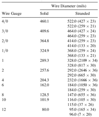
Table 2: Table equating solid wire gauge to stranded cable
EMC Aspects of Wires
While important, DC characteristics of wires are not the primary characteristics of concern in EMC work. The important elements to consider are:
- lines on a schematic (or connections in SPICE) that represent the “ideal” characteristics.
- frequencies of interest in EMC work that require an understanding of “non-ideal” behaviors.
A key consideration when using wires (or any type of conductor) with non-DC current is that there is AC impedance that increases with frequency due to the skin effect phenomenon. The skin effect causes a reduction in the cross-sectional area through which the current flows and, as we saw in a previous equation, the cross-sectional area decreases when the resistance increases. The same condition is a contributor to AC impedance. This is shown in the following figure and equation (Figure 6).

Figure 6: AC impedance of a conductor is composed of two parts: the DC resistance and the AC resistance (once the wire radius exceeds approximately two skin depths)
In addition, both the AC resistance and reactance of a conductor vary with frequency as a result of the skin effect, and are reflected in the resistance ratio factor (X).
DC Resistance, AC Resistance, and Inductive Reactance
If the fact that AC resistance can dominate DC resistance isn’t bad enough, since the wires are part of a current loop, they also have self-inductance and result in even higher impedance.
Table 3 summarizes these effects. It may even be startling that at only 1 MHz, the AC resistance is an order of magnitude greater than the DC resistance and the inductive reactance (XL) is hundreds of times the AC resistance!
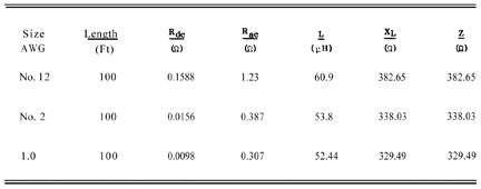
Table 3: Comparison of AC resistance, DC resistance and inductive reactance (due to partial inductance) for different wire gauges
Table 3 summarizes these effects. It may even be startling that at only 1 MHz, the AC resistance is an order of magnitude greater than the DC resistance and the inductive reactance (XL) due to the wire partial inductance as described in “Inductance: The Misconceptions, Myths, and Truth” is hundreds of times the AC resistance!
Figure 7 also shows the relationship between wire length, diameter, and its partial inductance. We can see that even “small” values of inductance (a few micro-Henries) have high impedance at EMC frequencies (due to X = jωL).

Figure 7: Relationships between wire length, diameter, and its partial inductance
Now that we have investigated the properties of single-strand wires, let’s look at the characteristics of stranded wires.
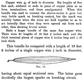
It turns out that an approximation can be made in that the resistance (and to a certain degree, self inductance — ignoring the effects of mutual inductance) of the stranded wire can be modeled as the resistance (inductance) of each strand divided by the number of strands (as each strand is effectively in parallel with the others). Interestingly, this was first empirically observed by Michael Faraday making the simple observation of “sparks” created in a circuit. When the same parallel wires were spread out, the “sparks” were less – without any change to the length of the wire bundle. Of course, we now know that fewer “sparks” mean less series inductance. Faraday’s observation is recorded as follows:
Wiring for Communication
As the 1800s continued, the “state-of-the-art” communications systems became the telegraph, and later the telephone, systems. As the infrastructure was developed and built for these, there became a need to understand, in detail, the physics of conductors (which were now called transmission lines). It was discovered that long distance communication paths had unique characteristics that hadn’t been seen before (Figure 8). This was because these installations were the first widespread development of large systems utilizing interconnecting conductors (wiring). This led to the development of the “Telegrapher’s Equations” (discussed later) that became the basis for transmission line theory.

Figure 8: Requirements of early electronic communications led to new understanding of conductors
….and Then It Happened – The First (and Still the Only TRUE) Ground Connection!
As the telecommunications boom of the 1800’s continued, more and more wire was needed to construct the systems. From this need, one fundamental of all electrical engineering procedures was born, the discovery that by using the earth as a current return path, only half the amount of wire was needed! Thus, the term “ground” was coined for electrical connections (Figure 9)!
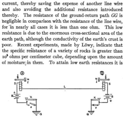
Figure 9: Early reference of the term “ground-return”
Analysis of the Ground Return
This practice for long distance telephone and telegraph connection was possible due to a unique physical relationship of the geometry and conductivity of the earth. It turns out that, rather than being a return path with a significant variation in impedance, the resistance reached an asymptotic limit just over 4 ohms (Figure 10).
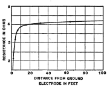
Figure 10: Graph showing the leveling off of resistance in a ground connection
This was due to the large area through which current could flow (similar to parallel wires) and, ironically, the resistance of the ground connection was much lower than the long signal wires. This further established the belief that a ground connection was a low impedance path (compared to the rest of the circuits).
Heaviside’s Discoveries: the Telegrapher’s Equations
An interesting phenomenon then occurred as the (telegraph) message signal speeds increased. It was discovered that some of the transmission lines caused signals to be affected and changed at the receiving end from their original characteristics at the sending end.
Heaviside then investigated Faraday’s observations of inductance, referenced Maxwell’s work, and from that work he developed the “Telegrapher’s Equations” which revealed how line characteristics affected signal propagation. This became the basis for all transmission line engineering.
This was amazing an insight. Heaviside realized that the use of two conductors in the telegraph transmission line resulted in the capacitive and inductive properties of the line. (This had not been recognized before.) He correctly understood that the capacitance and inductance are continuous along the length of the pair of conductors and therefore could be represented as either lumped or distributed components along the transmission line (Figure 11).

Figure 11: Heaviside realized that capacitance anc inductance are continuous along the length of a pair of conductors , and can be represented as “lumped” or “distributed”
We now refer to Heaviside’s work as the discovery of the Transmission Line Model (Figure 12). Most importantly, this discovery allowed for the describing of a transmission in term of its characteristic impedance (Zo), which is a function of the distributed inductance and capacitance along the line and which makes it independent of line length!

Figure 12: Diagram and equation for the Transmission Line Model
The Transmission Line Model
- Model that utilizes a line of distributed inductance and capacitance.
- Model that shows a line can be represented by a surge (or characteristic) impedance, ignoring small dielectric losses.
Transmission Line Signal Propagation
Key to transmission line theory is the ability to understand how energy, whether it’s “power” or “signal”, propagates along the line. A very good visualization of this is shown in Figure 13.
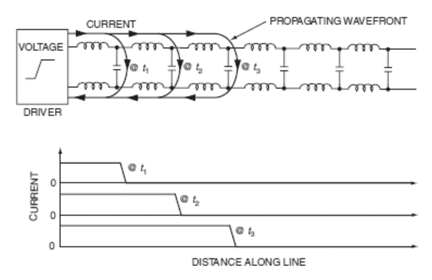
Figure 13: Illustration of how energy propogates along a line (courtesy of Henry Ott, page 218 of Electromagnetic Compatiblity Engineering)
As can be seen, the propagation essential takes place by the current flow through the line series inductance and the “charging” of the effective parallel capacitors. Since there is a time constant associated with the charging of the capacitors, this causes the propagation speed to be reduced compared to the traditional “speed of light” electromagnetic wave propagation through air/vacuum. The effect of this reduction in propagation speed is known at “velocity factor” and varies based upon the values of the inductance and capacitance (which is determine both by transmission line geometry and material used in the transmission line construction.
Examples of Common Transmission Lines
Today’s transmission lines are typically either coaxial or “twisted wire pair” (TWP) (Figure 14). Coaxial cable is used for shielding electrical fields and TWP is used for magnetic field shielding from emissions from either the transmission lines or from external interference.

Figure 14: A coaxial line is shown on the top and a twisted wire pair is shown on the bottom.
Other Types of Conductive Paths
A common practice is to utilize the metal chassis or enclosure as a conductive path (typically called “case grounding”) for either signal or power return. There are a number of reasons that this is done including:
- minimization of wiring costs (similar to telegraph “grounding”).
- resolve of component/system EMC problems.
Unfortunately, due to the fact that the impedance of the “ground” path is unknown, this results in the actual energy transfer loop being quite different from the “idealized” (previously discussed). The actual loop is shown in the Figure 15.
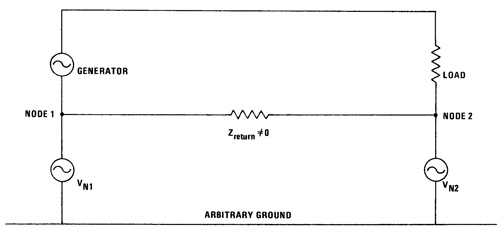
Figure 15
Implications of Practice
From that figure, it is easily seen that using the chassis or enclosure as an electrical return path would result in “ground” impedance being undefined and something other than the assumed zero (0) ohms. This impedance is comprised of two terms, the resistance (due to material and frequency) and inductance (due to geometry). Unfortunately, this would not be evident from looking at the schematic for the system and result equivalent circuit from this practice is shown in Figure 16.

Figure 16
Actual “Grounding”!
Since the chassis conductive path is very small (compared to earth) – there may be significant path impedance (Figure 16), resulting in unexplained “ground shift” conditions.
Signal “Grounding”
Connecting the signal return to the conductive chassis can cause undesired results due to impedance in the signal current path and/or the presence of other return currents (Figure 17).

Figure 17: Schematic of a signal return
Signal Return – Best Practice
The best solution is to isolate the signal return from conductive paths that are not well controlled or may have interfering currents on them (Figure 18).
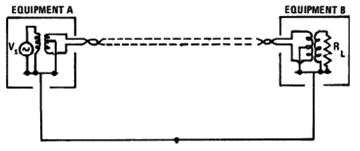
Figure 18: Isolation of signal return from the conductive path
Summary
There are undeniable realities of conductors that we need to be conscious of when working with circuits:
- Real conductors have properties of resistance and inductance that need to be considered.
- Conductors are the defined paths for the propagation of electrical energy.
- Wires can be either solid or stranded, with each having advantages and disadvantages.
- Transmission lines have inductance and capacitance that determine their characteristics.
And the moral is that any conductive path needs to be evaluated – not just assumed! ![]()
References
- Denny, H. W. (1983). Grounding for the Control of EMI. Gainesville, VA: Don White Consultants.
- Evans, R. W. (1997). Design Guidelines for Shielding Effectiveness, Current Carrying Capability, and the Enhancement of Conductvity of Composite Materials. Huntsville, AL: National Aeronautics and Space Administration (NASA).
- Hausmann, E. (1922). Telegraph Engineering – A Manual For Practicing Telegraph Engineers and Engineering Students. New York: D. Van Nostrand Company.
- Hopkins, W. J. (1893). Telephone Lines and Their Properties. New York: Longmans, Green, and Co.
- Ott, H. W. (2009). Electromagnetic Compatibility Engineering. Hoboken, NJ: John Wiley Interscience.
- Paul, C. R. (2006). Introduction to Electromagnetic Compatbility. Hoboken, NJ: John Wiley Interscience.
- Paul, C. R. (2008). Analysis of Multiconductor Transmission Lines. Hoboken, NJ: Wiley-Interscience.
- Raychem. (n.d.). Raychem Spec 44 Wire and Cable. Retrieved April 4, 2011, from Strancoproducts.com: http://www.strancoproducts.com/downloads/SPEC%2044%20WIRE.pdf
- Silver, Ward (Editor). (2010). The ARRL Handbook for Radio Communications. Newington, CT: American Radio Relay League.
- Thompson, S. P. (1898). Michael Faraday – His Life and Work. New York: MacMillan.
- United States Department of Defense. (1987). MIL-HDBK-419A: Grounding, Bonding, and Shielding for Electronic Equipments and Facilities.
- United States Department of Defense. (1998). MIL-HDBK-338B: Electronic Reliability Design Handbook.
- United States Navy. (1998). Navy Electricity and Electronics Training Series (NEETS) Module 4 – Introduction to Electrical Conductors, Wiring Techniques, and Schematic Reading.
This article is based on a presentation made during the “Fundamentals” workshop at the 2011 IEEE EMC Symposium and is an example of the type of material discussed at Fundamentals sessions.
 |
Mark Steffka, B.S.E., M.S. is a Lecturer (at the University of Michigan – Dearborn), an Adjunct Professor (at the University of Detroit – Mercy) and an automotive company Electromagnetic Compatibility (EMC) Technical Specialist. His university experience includes teaching undergraduate, graduate, and professional development courses on EMC, antennas, and electronic communications. His extensive industry background consists of over 30 years’ experience with military and aerospace communications, industrial electronics, and automotive systems.Mr. Steffka is the author and/or co-author of numerous technical papers and publications on EMC presented at various Institute of Electrical and Electronics Engineers (IEEE) and Society of Automotive Engineers (SAE) conferences. He has also written about and has been an invited conference speaker on topics related to effective methods in university engineering education. He is an IEEE member, has served as a technical session chair for SAE and IEEE conferences and has served as an IEEE EMC Society Distinguished Lecturer. He holds a radio communications license issued by the United States’ Federal Communication Commission (FCC) and holds the call sign WW8MS. |
