Foundations
When two circuits are in the vicinity of one another, a signal propagating in one circuit can induce a signal in another circuit, due to capacitive (electric field) and/or inductive (magnetic field) coupling between the circuits. This phenomenon is referred to as crosstalk. An example of such an arrangement is shown in Figure 1.
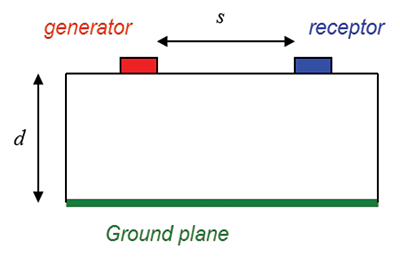
Two PCB traces in a microstrip configuration are separated from each other by distance s, and from the ground plane (which is return conductor for both) by a distance d. The first trace (generator conductor) is driven by a time-varying voltage source, VS with the impedance RS, and terminated by a load resistor, RL. The second trace (receptor) is terminated by the load resistors, RNE and RFE, on the near end and the far end, respectively. This arrangement can be modeled by the circuit shown in Figure 2.
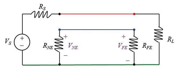
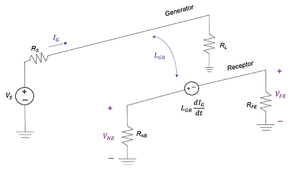
The time-varying current on the generator line, IG, creates a magnetic field that gives rise to the magnetic flux that penetrates the loop between the two receptor conductors inducing a voltage in the receptor circuit. We model this by the mutual inductance LGR as shown in Figure 3. (Note: this model is valid for electrically short lines, as we represent the induced voltage as a lumped source).
Similarly, the time-varying voltage between the two conductors of the generator circuit, VG, gives rise to the electric field lines, some of which terminate on the conductors of the receptor circuit inducing a current in the receptor circuit. We model this by the mutual capacitance CGR as shown in Figure 4.
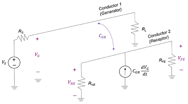
Superposition of the two coupling mechanisms results in the circuit shown in Figure 5.
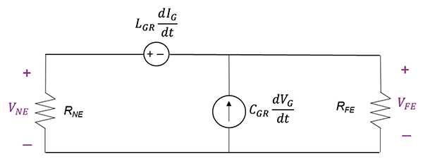
By superposition, the near- and far-end voltages are given by
 (1a)
(1a)
 (1b)
(1b)
Under the assumption of the line being electrically short at the highest significant frequency component of VS(t) the generator line voltage and current are essentially constant along the line. Thus,
 (2a)
(2a)
 (2b)
(2b)
and, therefore,
 (3a)
(3a)
 (3b)
(3b)
Thus, to minimize crosstalk we can reduce: 1) the variation of the source signal, 2) the inductive coupling, LGR, or, 3) the capacitive coupling, CGR.
Verification
The experimental setup for crosstalk measurements is shown in Figure 6.
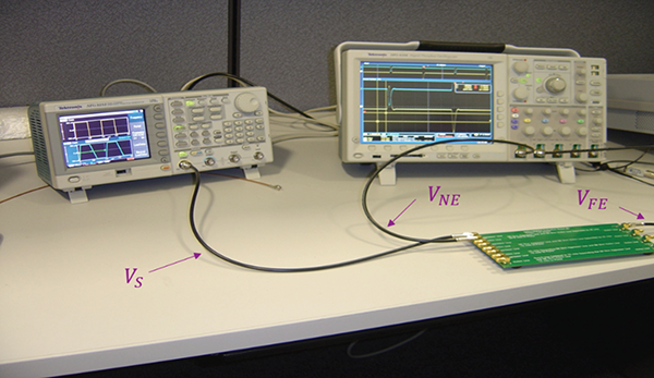
PCB with different circuit topologies is shown in Figure 7.

Three different circuit topologies were investigated, and are described in Table 1.
|
Case |
Line separation s [mils] |
Distance to |
|
1 |
25 |
54.8 |
|
2 |
25 |
12 |
|
3 |
75 |
12 |
Table 1: Circuit topologies
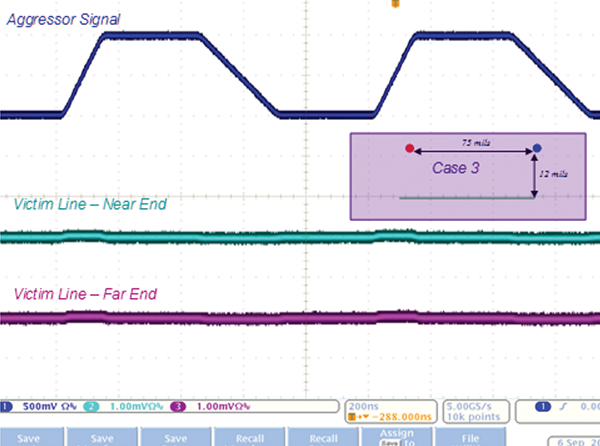
Figures 8 through 10 show the generator (aggressor) signal as well as the resulting near- and far-end voltages induced on the receptor (victim) line.
The source has an open-circuit voltage that is a 1-Vpp, 1-MHz trapezoidal pulse train having 100-ns rise time, 200-ns fall time, and a 50% duty cycle. We make the following observation in Case 1, presented Figure 8.
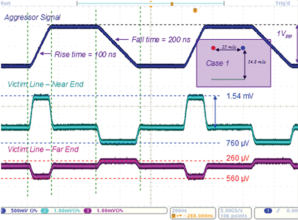
Voltage induced on the near end during the rise time is while the voltage induced during the fall time . Since the value of the rise time is twice that of the fall time, according to Equation 3a, the induced voltages should differ in magnitude by a factor of two, which indeed is the case. We also note that the polarities of the two voltages are opposite, which is to be expected from Equation 3a. Similar observations can be made for the voltages induced on the far end. Furthermore, since the coefficients of coupling for the near-end voltage (Equation 3a) are positive, the induced-voltage during the rise is also positive. The far-end voltage is negative during the rise time, indicating that the inductive coupling dominates the capacitive one (see Equation 3b).
Bringing the ground plane closer to the lines, while keeping the distance between the lines unchanged (Case 2), predominantly reduces inductive coupling and results in a reduction of the induced voltage magnitudes, as shown in Figure 9.
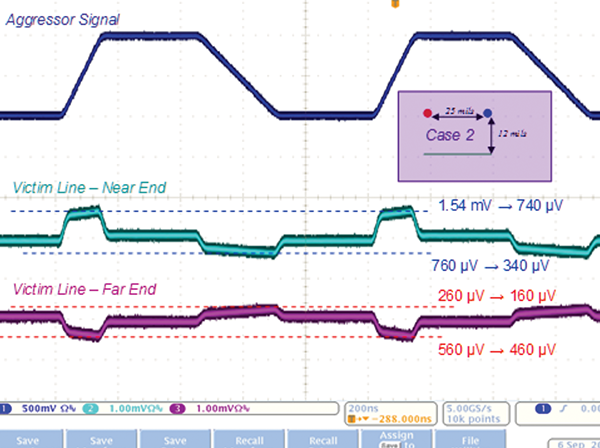
Case 3 depicts the scenario where the distance to the ground plane is unchanged from Case 2, but the separation between the lines is increased. This predominantly reduces capacitive coupling and results in further reduction of the induced voltages, as shown in Figure 10.
References
[1] Clayton R. Paul, Introduction to Electromagnetic Compatibility, Wiley, 2006.
[2] Henry W. Ott, Electromagnetic Compatibility Engineering, Wiley, 2009.
[3] Bogdan Adamczyk, Foundations of Electromagnetic Compatibility with Practical Applications, Wiley, 2017.
[4] Bill Spence and Pete Vander Wel, Designers of the PCB used for Crosstalk Measurements, Gentex Corp, 2008
