Introduction
There are many different opinions about the best decoupling capacitor strategy for printed circuit boards (PCBs). Different strategies for capacitor value, distance to the IC, etc. have been proposed and while there are good arguments of one or the other proposal, usually either will be effective, depending on some of the other factors involved.
It is universally agreed that the mounting of the capacitor on the PCB will increase the effective inductance of that capacitor sometimes by an order of magnitude or more from the equivalent series inductance (ESL). This greatly reduces the ability of the capacitor to effectively provide charge to the IC and lower noise between the power and ground-reference plans. Often many additional capacitors are added to give an effective, overall inductance that is acceptable.
This article will first explain the various portions of the overall inductance between the decoupling capacitor and the IC pins, then explore some alternative capacitor mounting approaches to reduce the capacitor’s connection inductance, which will significantly increase the performance of the decoupling capacitor in many situations. When these capacitor mounting approaches are effective, the total number of capacitors can be reduced without a decrease in performance.
Anatomy of the Inductance Impacting Decoupling Capacitor Charge Delivery
The main purpose of the decoupling capacitor is to provide charge (current) to the IC during the time the IC requires it. The main time-varying current draw for most CMOS ICs is when the IC is driving signals onto I/O traces on the PCB. Internal transistor switching, internal clocks, etc. usually are more of a constant DC current requirement at the IC power pins because of the internal package/chip inductance and capacitances.
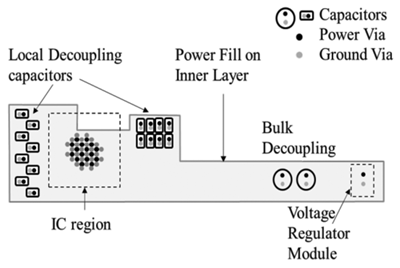
When the capacitors provide the charge the IC requires, the noise between the power and ground-reference planes is minimized and the effective impedance between the planes is low. The limitation of the impedance at low frequencies is the total capacitance and at higher frequencies the limitation is from the various portions of inductance in the current path. Figure 1 shows an example of a printed circuit board with an IC and some decoupling capacitors on the top and bottom of the power area. Figure 2a shows the impedance the IC pins ‘see’ looking into the PCB stackup for a couple of different cases of capacitors. The different curves are not important to this discussion, but it is clear that the low frequencies are dominated by the discrete capacitors and capacitance between the planes. Figure 2b shows the stack up for this particular PCB with the capacitance circled.

Switching to the very high frequency portion of the impedance plot, Figure 3a shows the impedance and Figure 3b shows that this is only due to the inductance the IC sees from the power and ground-reference vias between the IC pads on the PCB surface and the power and ground-reference planes in the PCB stackup (in this case, the planes are in the middle of the stackup). The inductance of this connection limits the effectiveness of the decoupling capacitors at the very high frequencies.
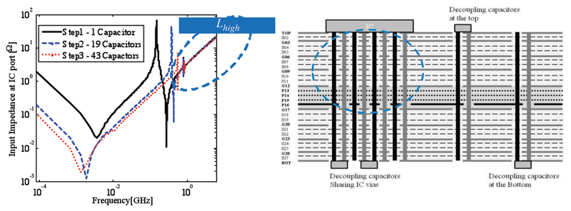
The center portion of the impedance plots is also inductive, but this inductance is more complex. It includes the IC via inductance, the inductance between the power and ground-reference planes, and the inductance of the vias connecting the decoupling capacitors to the planes. Figures 4a and 4b highlight this inductance. Minimizing this inductance requires the power and ground-reference planes to be near the top of the stack up so that the IC via inductance is minimized. Then the inductance capacitor vias can be minimized when the capacitors are mounted on the top surface of the PCB.

Minimizing capacitor via Inductance
Once the PCB stackup is defined, the discrete decoupling capacitors inductance can be further minimized with careful placement. The primary purpose of these discrete capacitors is to replenish the charge between the planes in time for the IC to draw more charge during the next cycle. Often designers will increase the number of capacitors hoping to reduce the inductance by adding more capacitors in parallel. However, it turns out that the apparent inductance seen between the planes and capacitor pads does not decrease as 1/N as might be thought. This is due to mutual inductance between the vias when the capacitors are closely spaced (as in common practice).
This mutual inductance can be cancelled for closely spaced decoupling capacitors by simply alternating the power and ground-reference pads on the PCB. Figure 5 shows an example of this alternating pattern. The red vias represent power, and the green vias represent the ground-reference vias.
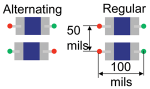
Figure 6 shows the inductance when the power and ground-reference planes are at the top of the PCB stack up and the separation between planes is 5 mils. The values of inductance are very low because the planes are at the top of the PCB stack up. To calculate the actual inductance when the planes are deeper in the stack up, simply multiply the inductance values by the number of additional 5 mil increments to get to the planes.
In the typical mounting case (regular) of the power vias in a straight line when the number of capacitors is increased. Figure 6 shows the inductance decreasing, but not as fast as a simple 1/N indicates. However, when the alternating geometry is used for the vias, the inductance falls off much faster than 1/N! If the target impedance required a decoupling capacitor effective inductance as represented by the dashed line, 30 capacitors would be required with the traditional geometry, while only nine are required with the alternating geometry. This saves not only the capacitors themselves, but the wiring channels that would be disrupted on all layers with the added vias.
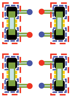
The effective inductance can be further reduced when two capacitors are mounted in a doublet fashion again with the power and ground-reference vias alternating (Figure 7). The effective inductance seen in Figure 6 is even less than the alternating configuration. In the optimized doublet configuration, the vias from each capacitor are placed closer together with short traces, while still maintaining the alternating power and ground-reference via configuration. This further reduces the effective inductance to the smallest possible value.
Summary
The inductive portion of the power distribution network (PDN) is limited by the inductance seen from the IC pads to the planes. However, the
actual inductance provided by the discrete decoupling capacitors can be reduced by cancelling the mutual inductance by alternating the vias. This reduction in effective inductance is greater than a simple 1/N decrease. Finally using a doublet of two capacitors, with the alternating vias, the effective inductance of the discrete capacitors connecting to the planes is further reduced.
Dr. Bruce Archambeault is an IEEE Fellow, an Adjunct Professor at Missouri University of Science & Technology as well as a IBM Distingushed Engineer Emeritus. He teaches short courses in EMI/EMC design and is the author of the book “PCB Design for Real-World EMI Control”.
Biyao Zhao is currently a Master’s Degree student at Missouri University of Science & Technology doing research in power distribution network design.
Dr. Ketan Shringapure recently graduated from Missouri University of Science & Technology where he studied power distribution network design. He now works at Apple Computer in California.
Professor Jim Drewniak is one of the lead researchers at Missouri University of Science & Technology and has a long history of publications in all areas concerning EMI/EMC.
