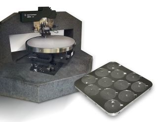
Agilent Technologies Inc. has introduced new 300 mm x 300 mm and multisample two-inch-wafer stages for its large-stage 5600LS atomic force microscope. These new stages extend the application versatility of the Agilent 5600LS AFM, which also offers the largest fully addressable and programmable 200 mm x 200 mm stage, plus a special stage adapter for imaging small samples.
“With its expanded selection of stages, the modular 5600LS provides researchers an ideal tool for semiconductor, optoelectronics, materials science and life science studies at the nanoscale,” said Jeff Jones, general manager for Agilent’s nanoinstrumentation facility in Chandler, Ariz. “The 5600LS is the world’s finest commercially available AFM that permits imaging of both large samples [in air] and small samples [in air, or in liquid under temperature control].”

The 5600LS system’s programmable, motorized stage quickly and accurately positions probes to image and map specimens with 0.5μm precision. Investigators can locate and identify an area of interest and, with the coordinates stored, automatically reposition the sample for further study. Multiple locations can be programmed. The stage easily accommodates either a single sample up to 200 mm in diameter and 30 mm tall or as many as nine small samples with the 200 mm vacuum chuck (more can be held with tape), each of whose locations can be programmed.
The new 300 mm x 300 mm stage allows 5600LS users to handle larger semiconductor wafer samples. Alternatively, the new multisample, two-inch-wafer stage is perfect for research involving optoelectronics and LEDs.
The 5600LS is compatible with all standard imaging modes and with Agilent’s unique scanning microwave microscopy (SMM) mode, which combines the compound, calibrated electrical measurement capabilities of a microwave vector network analyzer with the outstanding spatial resolution of an atomic force microscope. SMM mode is particularly useful for testing and characterizing semiconductors. It can be used to measure complex impedance (resistance and reactance) as well as calibrated capacitance and dopant density.
For additional information, visit www.agilent.com.
