
Conducted emissions negatively affecting an electronic system either through internally coupled emissions or from externally connected cables is of concern to hardware designers looking to either pass conducted immunity testing, or limit the electrical noise from their device. The result is a need to understand how electrical noise could conduct through a system. This requires an understanding of different types of noise currents, how to measure for them, and ultimately what type of suppression mechanism to use in order to get their product out of the door. Of course, they will need to do this by determining which suppression method is the most cost effective for the type of conducted emission they are getting.
In order to get a better understanding of what exactly conducted emissions are, we will first talk about the two types of emissions engineers will be encountering. After gaining a first principals understanding of those emissions, and how they can even affect radiated emissions, their paths and typical sources will be discussed which enables hardware designers to catch these problems in the design phase, so they avoid adding costly components in later phases of development. After identification and understanding of the problem, the next most important topic is how to measure these emissions. This is where engineers will encounter these two common devices during testing, either a directional coupling network for injected immunity testing or a line impedance stabilization network (LISN) for emissions measurement. Finally, after understanding how to measure, we will discuss filters and components for different applications.
At the end of the article you should have a good understanding of what conducted emissions are, their sources and paths, how to measure for them, and lastly how to control them at different stages of design.
Conducted Emissions and the EMC Model
Most if not all of us have experienced problems in conducted emissions be it via an alternator whine on your vehicle stereo system, or a vacuum cleaner interfering with your television. Because of that its import to understand where on the EMC model of source-path-receiver, that conducted emissions fit into to quickly remedy an issue.
The source of most conducted emissions issues is classified as either those coming from outside the system, and those from inside or locally to the module or system being tested. Because of this, you will find a lot of conducted emissions material targeting filter design and wire routing to try to reduce the effect the noise source has on the system. An example of this, described earlier is an alternator creating an unintended noise current as the result of its power generation described in Figure 2.
This noise current may vary with the engine speed and could result in negatively affecting radio performance, either via a conducted or radiated path. While you may think that the noise source is normally easy to target, as it has characteristics that include harmonic content, or high amplitudes the path this noise takes is often difficult to follow. Examples of these types of paths are usually the result of an unintended coupling mechanism such as a poorly grounded cable, a conductive chassis, or parasitic capacitances that arise from something as benign as a heat sink on a transistor. Figure 3 demonstrates an example where an off-the-line switching converter is being driven at 150 kHz, the dotted line capacitor representing a parasitic capacitance that exists between the heat sink and the ‘ground.’
The red line represents the path the noise current can take, and brings in a device that will be touched on later called a LISN that will help measure the voltage created by this conducted current. It is also important to remember that in Figures 2 and 3, the path includes a radiated path either onto an antenna and into the stereo amplifier or to a conductive chassis.
In order to control conducted emissions we must first create some rules that will help us to identify the type of conducted emission so we can identify the source and filter it, or the path and either reroute or otherwise modify the system such that it no longer is an issue.
Types of Conducted Emissions
The first step in dealing with conducted emissions issues is to first identify how the noise path is being transmitted through your system, either via the operational current path (loop) or by an unintended current path (radiated or along the common line). Therefore, conducted emissions are then classified based on the condition that created it and as such result in different remedies.
Differential Mode
The first type of noise current that appears in series with operational current is referred to as the differential mode current or differential mode noise. A common diagram usually shown when describing differential mode noise is referred to in Figure 4, where in a traditional three-wire system the noise source is depicted along across the load. The differential mode current here creates a noise voltage referred to as in series with the hot and neutral lines; in non-three wire systems, these would be considered the signal and return lines. It appears in series with the operational current and as its name suggests is differential in nature.
Luckily, when debugging differential mode problems it is usually straightforward since it is in series with the loop current and as such, the clues to solving the problem can be found by carefully analyzing a schematic for things such as:
- High equivalent series resistance (ESR) capacitors creating a voltage drop when transferring charge from the capacitor to the source such as a microcontroller, amplifier rail, or the output filter on a switch mode power supply. A simple example of the ESR of a capacitor creating a voltage drop is shown in Figure 5.
- High frequency transients from any number of harmonic rich content that exist in electronic systems today such as switch mode power supplies, high speed digital communication lines such as I2C or SPI, and control signals.
- Traces that are undersized for the current in which they are intended to carry (high equivalent resistance) or are too long (high inductance) and thus create an appreciable voltage drop during transient operation.
Common Mode Noise
After referring to differential mode noise currents as noise currents that flow in opposite directions, then it makes sense the refer to the converse where the noise currents appear in the same direction; since the emission is common to both the signal and return path it is referred to as common mode noise. To help visualize this situation, we again refer to a simple three-wire system in Figure 6; here you will find the noise voltage because of noise currents appearing across true ground- a path not normally carrying current. The common mode current here appears on the ground common to both the hot and neutral lines.
Unfortunately, this type of noise current is more difficult to identify, as it is very sensitive to the path that the noise currents take. Their path usually involves parasitics and does not relate to the normal operational current flow, and as such does not show up on a schematic. In Figure 7, you will find an example of how the common mode path can propagate in a two-wire system involving two transistors, and a DC/DC converter driving a load in a floating metal housing.
Common mode noise problems are a headache for designers, and usually part of a physical problem such as:
- Poor ground scheme in a printed circuit board layout where the return path designed by the ground plane is of higher impedance than the common mode path;
- Poor shield termination usually in the form of a high impedance pigtail instead of a low impedance BNC termination; or
A poorly grounded harnesses.
In addition, while they are capable of showing up in the large majority of electronic systems they are usually most likely to cause headaches in:
- Audio systems where any sort of noise on the common mode path could create an audible hum through a speaker or microphone;
- RF and antenna systems where they could affect the currents on the antenna element, and for this reason they are sometimes referred to as the antenna current; and
- High power switching power supplies.
In addition, the common mode path is usually the culprit for the majority of radiated emissions problems as well, since the current loops made by noise currents taking this path tend to be larger than differential mode.
Of note when debugging and trying to analyze the path the conducted emission is taking it is important to understand that common mode and differential mode problems are not mutually exclusive situations. Differential mode current that is unbalanced across the source and return path can present itself as common mode noise, for example. In addition, because of this, the most efficient way to manage the problem is suppression at the source, which involves paying attention to common noise sources:
- Noise associated with the supply – This would include common and differential mode currents generated by the power supply, or something coupled to the input power.
- Noise associated with common noise sources – This would include a bus (memory, or SPI), PWM, or clock signals that with return currents traveling through an unintended path.
Without careful analysis filtering and suppression techniques used to reduce one, can result in an increase for the other.
Conducted Emissions as Radiated Problems
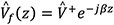
Before discussing how we measure conducted emissions, it is important to understand that common and differential mode currents are not just a hardware problem but they also relate to the radiated electric field. Excessive amounts of either, or both, can cause a device to fail radiated emissions testing in addition to giving operational problems. To control common and differential mode currents, we first must understand how these currents relate to the measured field. A common equation we can use to estimate differential mode radiated emissions a differential mode current with the following formula:
![]()
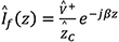
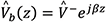
It is important to note that since differential mode currents are loop currents, the emissions they generate are linear with the area of the loop they travel. Conversely, the field generated by the common mode current is given by:
![]()
In both these equations, we notice a dependency upon the frequency and two constants. These constants are about an order of magnitude different:

If we consider both the differential and common mode currents in a system to be contributors to noise in a system we should note that the field coming from a common mode current is much stronger than that of a differential mode one. By using some algebra to simplify the equations by setting the lop area to , a wire length of , and the frequency to 48 MHz we can get a sense for how the common and differential mode currents relate to each other; this is shown as follows:

This equation tells us that for this set of simplified parameters, a single micro amp of common mode current can produce the same field generated by a milliamp of differential mode current.
Measurement Techniques
Now that we have discussed the different types of noise sources, their drawbacks and gave some examples the next logical step in going about fixing them is figuring out how to evaluate them. Evaluating the effects noise has on a circuit, as well as the emissions coming from a device brings about two common devices, the first of which being a LISN. The LISN is used for measuring the conducted emissions coming from the device under test, and ensures repeatability between test setups and isolation from the variability of outside noise. The second is the directional coupling network (DCN), which is used for evaluating how your device under test reacts to conducted emissions, usually referred to as injected immunity testing. Here instead of measuring noise, the test is designed to see how the device reacts to varying amounts of injected RF noise imposed upon the AC mains of a device.
The physical setups, specifications, and details behind the test setups for each of these devices vary from industry to industry.
Introducing the Line Impedance Stabilization Network
First, we will discuss the LISN as a valuable device for measuring the emissions coming from your device; its main goal is to have a constant line impedance over the range of measurement frequencies of interest. An example of LISN impedances where the impedance is not a constant 50 Ohm until 1 MHz is shown in Figure 8.
| Frequency | Equivalent Impedance (ohms) |
| 10 kHz | 5.36 |
| 20 kHz | 7.25 |
| 40 kHz | 11.99 |
| 50 kHz | 14.41 |
| 100 kHz | 25.11 |
| 200 kHz | 37.74 |
| 500 kHz | 47.21 |
| 1.0 MHz | 49.26 |
| 2.0 MHz | 49.80 |
| 5.0 MHz | 49.98 |
| 8.0 MHz | 50.00 |
| 30.0 MHz | 50.00 |
Figure 8: Example chart of a LISN and its impedances vs. frequency
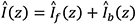
Since the LISN is meant to isolate the device being tested from the powerline impedance variability and provide a measurement port, it sits in line with the input power and separates the power current from the noise current as well as blocks any external noise currents from corrupting the measurement. Shown in Figure 9, this block diagram details where the LISN exists in relation to the product and commercial power system.
Taking a closer look inside the LISN, we will find a low pass filter made up of inductors and capacitors. Looking closely at this diagram, and back at Figures 4 and 6, you will notice that the LISN measures both common and differential mode voltages from its measurement port.
The values of the components inside the LISN while similar are not the same across different industries and different frequency ranges. This is due to each specification and regulating body requiring different stabilized impedances specific to the environment they operate in; however, there are some common ones shown in Figure 11.

The LISN allows the tester or designer to see if the emissions coming from their device comply with the ever-growing number of regulatory bodies, or if additional work needs to be done on power supply filtering. However, if you want to see what happens in the presence of a conducted disturbance from somewhere else on the commercial power system, from for example a motor turning on/off, the directional coupling network is the device to test your immunity.
Introducing the Coupling Network
Measuring how your device works under disturbances is useful across a wide range of applications. From automotive, where designers have to ensure an alternator dumping current into your vehicle system will not damage electronics, to commercial systems where you want to ensure your stove does not turn on every time the refrigerator does. For the purposes of this article, we will focus on the International Electrotechnical Commission (IEC) standards of testing for commercial and industrial usage defined in the 61000 series tests. IEC is the governing body that sets forth a generic setup that covers conducted and radiated disturbances across a wide range of test criteria in its 61000 series testing. The two that relate to the content in this article are:
- 61000-4-16, which tests for immunity to conducted common mode disturbances in the frequency range from 0 Hz to 150kHz; and
- 61000-4-5, which tests for immunity to conducted disturbances induced by radio frequency fields from 150kHz to 80MHz.
These tests subject the device to disturbances in both common and differential mode setups and are most useful for devices with at least one conducting cable such as a: Main’s supply, signal line, measurement line, or an earth connection connecting to another system. They are meant to expose weaknesses in your product to common noise sources such as PWMs, Clocks, and Relay chattering that could find their way into your system. The block diagram for an immunity test looks similar to Figure 12, where you have a signal generator, amplifier, and directional coupler that work together to deliver a constant noise signal modulated on top of the normal AC mains.
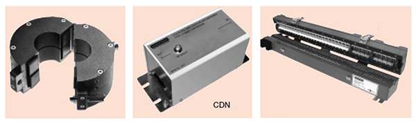
In some higher end systems, a power meter and computer controller is used to both measure and control the amplitude of the injected disturbance to account for RF losses in the system over the range of interested frequencies. For the 4-6 series of testing the amplitude of the injected noise is to be kept constant at either 1, 3 or 10V depending upon the level of certification wanting to be tested to. Unlike emissions measurement, this testing can be nuanced depending upon the industry you are in as the acceptance criteria is based upon your choosing and IEC simply outlines the testing requirements and methods. For example, you may want your device to function properly at 3V of disturbances while under operation, but at 10V the device may just not need to malfunction in an ambient condition. In addition, not all directional couplers are the same and come in a variety of flavors to fit your application, examples of common ones are shown in Figure 13.
After measuring the performance of your device, and like most you find an issue, the next step is to figure out what you can do to filter or suppress spurious emissions such that your product can be sold.
Filtering and Other Suppression Techniques
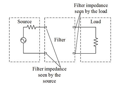
Attacking conducted emissions early on and in the most efficient way possible is the best way to avoid costly changes late in the design process. For this reason, after evaluating your system early in the development process and upon finding a problem we have to ask ourselves- Is this a common mode problem, or differential mode problem? Each type of emission has its own suppression mechanism, and the fixes can range from cost sensitive techniques such as a better layout, or filter to more last minute devices such as expensive chokes, ferrite beads, and cabling. In either situation, the goal of any filter is to affect the impedance of the path of current by causing a mismatch between the impedance of the noise source and the path that is affecting the receiver.
We will first start with filtering; something that many engineers are familiar with since they first learned about that first order low pass filter can clear up noise from a motor or microprocessor. The goal of a differential mode filter is to provide an impedance mismatch between from the circuit to the filter, such that the filter will absorb or redirect the noise away from the load.
These filter components usually consist of series inductance and parallel capacitance, and can be designed to have minimal impact upon desired current as long as the source and load impedances are taken into account in their design. To aid in understanding how the impedance of these reactive elements help to filter it helps to think of capacitors as being a high impedance (they contain an open circuit) and conversely inductors as being of low impedance (they’re made of bare wire). With this knowledge Figure 15 depicts how these elements can form primitive to advanced filters such as the PI or T network found in many line filters.
When choosing the type of components to use, it is important to keep in mind component and lead parasitics can play a large role in the performance of these filters, and often a spectrum analyzer with a tracking generator can be an invaluable tool in the evaluation of the insertion loss of these filters.
While differential mode filters are among the most familiar differential mode filtering components, the most ubiquitous common mode example are likely chokes and ferrite beads. Moreover, as their name suggests these components only effect the common mode current path by presenting a large impedance to currents traveling in the same direction. A diagram shown in Figure 16, demonstrates how the common mode currents create canceling magnetic fields while the differential mode currents are allowed to pass through the ring choke without attenuation.
Other examples fit over power lines (such as the small device attached to your laptop cord), but are always found closest to the noise source; examples are shown in Figure 17. The effective range of frequencies and attenuation level for each device depends upon the ferrite material and number of turns the wire has through the choke.
It is important to note that their last minute effectiveness comes at a cost- price and reliability, as they are usually expensive parts and can fall off.
As stated previously, while a clever layout can negate many problems the power supply front-end filter is where your dollar can be most effective at reducing noise. Now that we have introduced chokes and differential mode filters, we can put them together to form a power line filter. An overview of the filter is shown in Figure 18.
While this may be a lot to look at, we can break it into its two components- first the differential mode component as shown in Figure 19.
This section of the filter is made up of one or more differential mode capacitors across the power and return line and shunts any high frequency noise that may be in series with the power current back to the source. This capacitor is referred to as and is usually large with respect to the common mode capacitors . It is important to note here that there is some leakage inductance caused by imperfect coupling in the next stage of the filter, the choke.
The common mode section of the filter is made up of a common mode choke and utilizes line bypass capacitors to give a low impedance path of any common mode noise from the power supply or device, back to its source. An example is shown in Figure 20.
While filters are needed, hardware engineers should pay attention to routing, termination, and parasitics throughout the design phase to maximize filter effectiveness.
Conclusion
I hope that this article has inspired you to go tackle your next conducted emissions problem by giving you an overview of the two paths noise can take. The first being via differential mode and it involves the operational current in the circuit, which means it follows a documented path and can be solved through system analysis of the schematic, layout, and component choices. The second is via the common mode, which is usually caused via the unintended path provided by component parasitics such as heat sinks, or poorly terminated wiring harnesses. Here the engineer must focus on the source and paths in order to solve the problem. LISNs and directional coupling networks are common devices used to measure the performance of your product, such that when it comes time to design a filter it is being done to maximize effectiveness and early enough such that the cost increase is nominal.
 Christopher Semanson works at Renesas Electronics America Inc. as an Electrical Applications Engineer in Durham, NC supporting a wide variety of general purpose applications. He has five years previous experience in EMC Education at the University Of Michigan, teaching EMC and Electronics with Mark Steffka. He has a bachelor’s degree in Electrical and Computer Engineering and a master’s degree in Electrical Engineering from the University of Michigan Dearborn. Chris can be reached at christopher.semanson@renesas.com.