Practical Guide for Factory Engineers and Technicians
Why Measure EMI in Real-Life Applications?
For EMC practitioners the most important EMI measurements are in the test laboratory to verify EMC compliance of an individual piece of equipment with applicable Standards. However, there is a life after the laboratory, one full of real-life EMI adventures. The whole reason for an EMC test in the lab is to assure low, or acceptable enough, levels of EMI in the actual product’s use.
The problem is that the lab measurements have very little to do with real-life applications1. This article will focus on measurements of EMI levels in that actual use, more specifically, conducted EMI.
Semantics: while EMI is often defined as a process of interference with, or disruption of operation caused by high-frequency signals, in this article we will bend this definition a bit for brevity sake and use it as a convenient abbreviation for high-frequency signals that cause such problems.
Manufacturing Process
What are the EMI-related needs of manufacturing, or, for that matter, most of real-life applications? The key concerns are the throughput, high yield, low cost, and product’s reliability. Strong EMI presents at least the following impediments to the above:
- Equipment downtime, i.e. interruptions in operation of production equipment;
- Errors in measurements, often leading to altered process parameters in automated production;
- Errors in data communication; and
- Exposure of sensitive devices to electrical overstress (EOS)2 which lowers yield and increases probability of product failure in the field (latent damage).
EMI performance of any one particular tool isn’t as important as the overall EMI environment in the process which encompasses all the equipment in the process plus EMI from the facility mains and ground. We will focus on the complete approach to EMI that is focused on the process, not on individual equipment.
Most EMI signatures in real-life applications are transients, i.e., short pulses, periodic or not. Our instrumentation and methodology will be focused on this type of signal.
Worst Case
EMI is generated by operation of equipment in which operation is likely to be intermittent and/or seemingly random. One needs to practice patience and determination to capture the highest signals. Make sure that your equipment is fully operational when making measurements. Set your oscilloscope’s triggering to Normal and keep raising the trigger level until triggering stops; then wait for a minute or two just to make sure that you didn’t miss a big event. The worst case will eventually happen whether you tried to capture it or not, so you may as well make an effort to capture it.
Conducted Emission
This article focuses on conducted emission – any type of unwanted high-frequency signals present on wires and other conductors in equipment or a facility with all equipment operational. For EMC practitioners this is a departure from traditional conducted EMC tests that focus solely on EMI on power lines of individual equipment. So, if EMC regulations are zeroed in on only power lines, why then would we want to measure EMI on anything else than power lines?
One of the key sources of EMI-caused problems resides not on live and neutral wires of AC mains but on ground. This includes both facility ground and grounding inside the equipment. At high frequencies there can be voltage differences between different grounded points inside equipment even if the resistance at DC or impedance at the mains’ frequencies (50/60 Hz) is very low. This paper3 shows high-frequency signals with peak amplitude exceeding 1V between grounded points with impedance of just 0.2 Ohms between them. At high frequencies impedance is quite a bit higher than at 50/60Hz due to parasitic inductance of wires and skin effect. High impedance at high frequencies inevitably leads to voltage difference causing problems with reference points for electric circuits and electrical overstress exposure for sensitive devices assumed to be safe when contacting grounded surfaces. Another conducted EMI problem – high-frequency voltages and currents on data lines – is often caused by induced signals on runs of data cables.
EMI on Power Lines
First and foremost, mind safety! Any measurements on live power lines carries risk. If you don’t have proper qualification on working with the mains’ voltage, please take appropriate courses and/or involve a licensed electrician to assist you.
Measurements of EMI on facility power lines reflect total EMI “dumped” on the shared facility power by a combination of all equipment in the facility. Measuring EMI presents several challenges.
High Voltage Problem
Connecting your oscilloscope or a spectrum analyzer directly to a live power line is never a good idea. The peak voltage on a 250VAC line reached 353V in each polarity, requiring at least a 100:1 probe. Even with such a probe, strong power line surge can still damage your instrument. EMC laboratories use a specialized tool – LISN (line impedance stabilization network)4– that is supposed to emulate a real-life power line in the laboratory conditions. LISNs have a high-pass filter (just an L-C network) to provide signal output free of mains’ frequency. One of the problems is that we are already working with real power lines and the LISN will cause errors in frequency response by unnecessarily “doctoring” line impedance5. Another problem is that the LISN provides hard connection to ground which causes ground loops in measurements and a potential safety hazard. This makes a LISN unsuitable for use in our applications.
Ground Loops
Most oscilloscopes and spectrum analyzers are AC powered and thus grounded via their electrical plugs. If during measurements the ground lead of your scope probe touches live wire, this would cause a catastrophic short via your instrument; if the scope probe’s ground touches any other ground in wiring or equipment, this would create ground loop with serious measurement errors as the best outcome. Battery-powered instruments alleviate most of these problems, but not all.
Measurement Problem
When connecting your instrument directly to a power line using 100:1 probe, this probe attenuates not only power line mains voltage, but all signals on power lines. High-frequency signal will also be reduced 100 times making it difficult to measure. If you are concerned with noise of 0.3V as specified in IPC-A-610 (see further in the text)6, now you would have to deal with looking for a 3mV signal with dubious certainty.
Triggering Problem
If the above is not enough, it is unlikely that you will be able to trigger your oscilloscope on the elusive high frequency signal because your oscilloscope will be latching on an overpowering 50/60Hz signal. Even the oscilloscopes with high-pass filter on trigger are unlikely to succeed because the ratio between peak level of AC mains and high frequency noise is just too high.
Impedance Matching
A 100:1 probe coupled with the scope would inevitably have high input impedance which is a poor match for the impedance of high-frequencies source on power and ground wires. This would cause ringing of high-frequency signals and amplitude errors.
A Better Way to Measure EMI on Live Power Lines
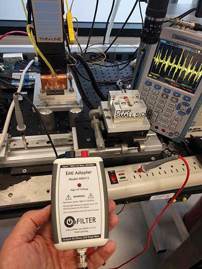
These problems can be solved with specialized power line EMI adapters (an example is shown in Figure 1). Such adaptors typically provide the following features:
- Galvanic separation from power line
- Balanced input
- 50 Ohms output
- Flat frequency response within the required range
- Overload limiter to protect other instruments
With these adapters one can safely measure EMI on live power lines without any artifacts.
Ground EMI Measurements
When measuring EMI on AC power lines the first check is whether the outlet is wired properly – all too often ground and neutral are reversed (regular three-LED checker doesn’t check for that) and return current flows through ground, not through the neutral. Besides being a safety violation, this facilitates strong EMI. To identify this problem, take a regular AC clamp meter and measure current through ground conductor in an electrical distribution box. There is always some AC leakage current, but it should be limited. If you see AC current over ~0.5A on ground, start asking questions. If this current reaches several Amperes, you can be certain that at least one piece of equipment connected to this power branch has neutral and ground reversed. You can diagnose it by measuring current in ground leading to one machine at a time. Involve a safety specialist at your company and correct this problem before addressing any EMI-specific issues.
We already know that there can be significant high frequency voltage between two otherwise well-grounded points. Why is this bad? In short, problematic reference voltage for electronic circuits and a possibility of electrical overstress. This is well covered in literature2,8. In this paper we will focus on measurements. Measurements of voltage between different grounded points using an AC-powered oscilloscope are worthless because an oscilloscope’s own ground connected via its AC cable to the mains’ ground adds yet another variable to this equation. A battery-powered oscilloscope or any oscilloscope with the EMI adapter described above is a better way of measuring EMI between different grounds. User should be careful when using just the battery-powered oscilloscope alone because sometimes the presumably grounded object isn’t really connected to ground and has rather high AC voltage – it pays to check before connecting your oscilloscope. If you are using an EMI adapter this is not a problem because it galvanically separates mains’ voltage from its output.
Where to Measure?
In short, where it matters. Traditional EMC tests cover emissions only on the outside of equipment – this is by far insufficient for real-life use. EMI causes problems everywhere, mostly inside the equipment. We will consider as examples the following cases: AC mains, facility ground, automated handling process, and manual soldering.
AC Mains
Please review notes about measurements on EMI on mains earlier in this article for safe and accurate results.
EMI on power lines can be differential (between Live and Neutral) and common mode (between Live or Neutral and Ground). The nature and the pattern of such emission are different – both need to be measured. You may find situations with plenty of differential EMI and very little common mode one, or just the opposite. A good portion of EMI on mains (except occasional commutation events – On/Off) are synchronized with the waveform of the mains’ voltage.
Make sure that the equipment is fully operational when performing the measurements – equipment in “Off” state produces no EMI.
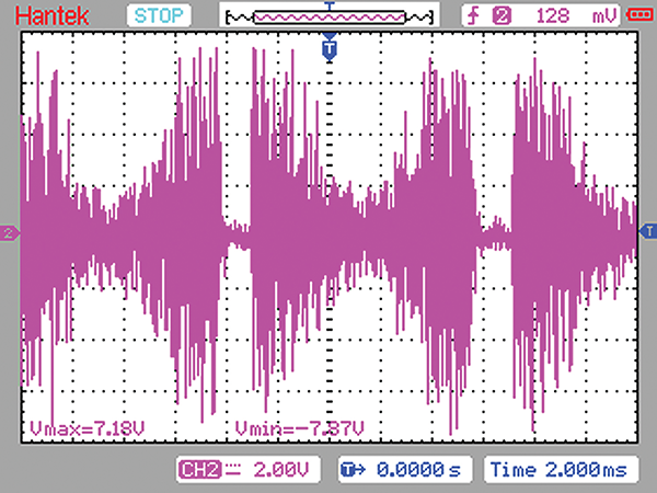
As an illustration, Figure 2 shows EMI at the output of uninterruptable power supply (UPS)9. In short, this is EMI from operation of a switched mode power supply (SMPS). Note how it is synchronized with 60Hz mains.
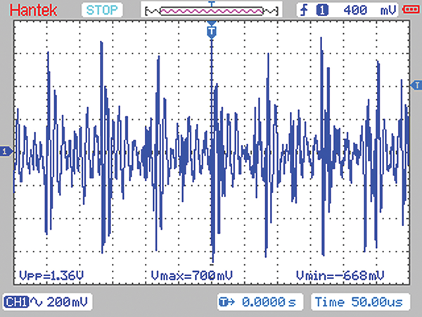
Some factories have separate facility ground – either a separate ground cable or ground bars. One of the reasons for such separate ground is potential reduction of EMI. This assumption sometimes fails spectacularly. Figure 3 shows EMI voltage between such “special” ground and the mains’ ground. A piece of equipment or a workbench connected to both grounds may have a hard time with reference voltages for its electronics and with exposure of devices to EOS.
In manufacturing, different tools often are conjoined for performing a task. It helps if there is no EMI voltage between grounds of these tools. AC powered oscilloscope by itself, of course, is not the right tool for such measurements.
Measurements of EMI on ground or between grounds of different tools can also be done using a current probe, but only after verifying that both grounds are actual grounds.
Automated Handling Process
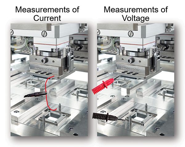
Figure 4 shows points of measurements of EMI between the robotic arm and the chassis of an IC handler (same applies to other tools handling semiconductor devices such as SMT pick-and-place machines, wire bonders, die attach, etc.). The assumption that a device is “safe” when in contact with ground and nothing else fails a basic equipotentiality test – the voltage difference between different grounded points at high frequencies may not be zero10.
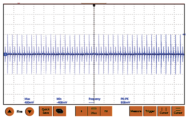
Figure 4 depicts actual voltage measured in the setup of Figure 5. As seen, the peak voltage (the one that matters – not RMS) is 400mV – higher than applicable Standards – we will look at these Standards further in this article.
Manual Soldering
From an electrical overstress aspect, soldering is one of the worst processes one could imagine – a metal tip of the soldering iron makes a galvanic connection to the pins of the devices which are connected to a potentially different voltage point. The soldering iron tip is grounded via AC outlet; PCB is coupled to the bench ground which is often connected to so-called “ESD” ground. When the tip of the iron touches the component, resulting current can easily subject device to electrical overstress. Whether the PCB is galvanically connected to ground or capacitively coupled to it, this can still happen because capacitive coupling offers very low impedance to high frequency signals11.
How should we test for EMI-caused EOS in a soldering process? Figure 6 provides some suggestions – voltage (a) and current (b and c) measurements. A user is advised to put together a kind of a fixture as shown to avoid burning fingers or melting test probes. The resistor in Figure 6c is 10 Ohms (any value between 10 and 50 Ohms will do).
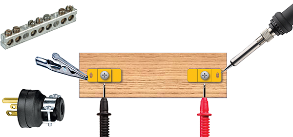
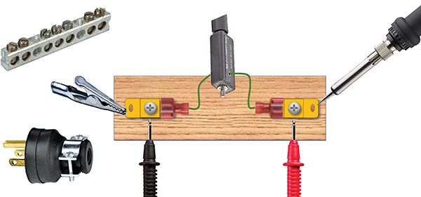
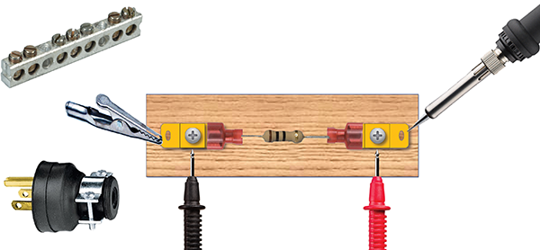
The left terminal of the fixture should be attached to either AC ground via power plug or to the ground bar on the workbench (verify first that it is indeed grounded).
The probes shown belong to an EMI adapter that resolves ground loop issues. An oscilloscope without it would work only if it is battery-powered, otherwise the measurements would be completely meaningless.
What if the EMI is caused by a soldering iron itself? Absolute majority of professional grade soldering irons do not introduce high-frequency artifacts by themselves. The problem lies in EMI on the facility’s AC power and ground.
Figure 7 demonstrates this cause-and-effect. The current spike from the tip of the iron is well-synchronized with the corresponding spike on the mains (as measured with an EMI adapter so that the oscilloscope is well-insulated from the mains).
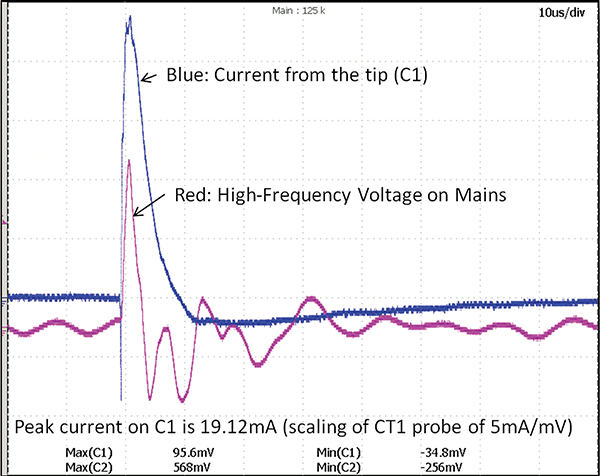
Is what we see in Figure 7 safe for the devices? This will be discussed further in this article.
Measurements of Voltage vs. Current in Ground
For operation of electronic circuits, having identical voltage reference in a distributed architecture is most important. For EOS exposure, both voltage and current measurements are meaningful, although, ultimately, it is the current that causes EOS damage, voltage measurements are also quite adequate. From the safety point of view, current measurements between two unverified grounds may cause short circuit should one of the presumed “grounds” be not a ground at all – always verify that assumed “ground” is indeed ground.
Figure 5 shows how to measure current between robotic arm and the tool’s chassis. A special current probe should be used for this purpose. The bandwidth of such a probe should start at low kHz and extend to at least 30MHz. The probe’s sensitivity to 50/60 Hz is a detriment as it masks the signals of interest.
How to Measure
The only meaningful measurements can be obtained on a working tool. This presents both safety and functionality problems. It is not only unwise but outright dangerous to have your hands in the midst of moving robotics. When performing measurements inside equipment always work together with the person in charge of that particular tool. Instead of putting your hands inside the working tool, utilize jumper wires with alligator clips with enough service slack that won’t interfere with movement.
A metrology purist at this point would note that all these wires will adversely affect the measurements and will be highly susceptible to radiated emission which is always plenty in a manufacturing environment, especially inside the equipment. That purist would be correct. But the only alternative would be not doing the measurements, so we will accept inherent unevenness in frequency response and signal ringing as a “fact of life.”
Dealing with Radiated Emission Interference
High-frequency signals on wires and metal objects mean corresponding high frequency radiated emission as well. Such electromagnetic fields induce unwanted signals into test leads and corrupt measurement results. To see if your measurements are affected by radiated emission grab the test lead with the palm of your hand – if the readings change, radiated emission is certainly a factor and is likely added some mV or mA to your data. Allow for it when analyzing your results.
Instrumentation
While from EMC regulations’ point of view, signal levels at a particular frequency are a measure of either passing or failing the requirements, for most cases in the field it is the peak value of a total signal that is of importance. A transient signal most common on power lines may have wide spectrum with signal amplitude spread across it, but this is not what matters – the peak value of the pulse does. Therefore, in absolute majority of cases frequency-domain measurements are not as important as time-domain measurements. And the best tool for that is a digital storage oscilloscope. Some real-time spectrum analyzers offer ability to analyze some transients, but are still too slow for the task. Conducted emission do not require high end oscilloscopes – 200MHz bandwidth with at least 1GS/sec is quite sufficient.
Settings of Oscilloscope for EMI Measurements
Incorrect measurements may lead to decisions that could be expensive and difficult to correct. Let’s assure that our measurements are done well. Proper settings of an oscilloscope improve our chances of doing so. The majority of EMI signals on power lines and ground are transients, i.e. pulses, therefore we need to set the scope up to capture and correctly measure such signals.
Vertical Scale
Figure 8 shows a signal displayed using different vertical scales. Not only the visual waveforms are quite different, measured numbers are different as well. Yet, it is the very same signal. Why such a difference?
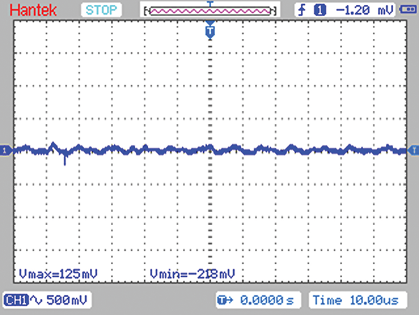
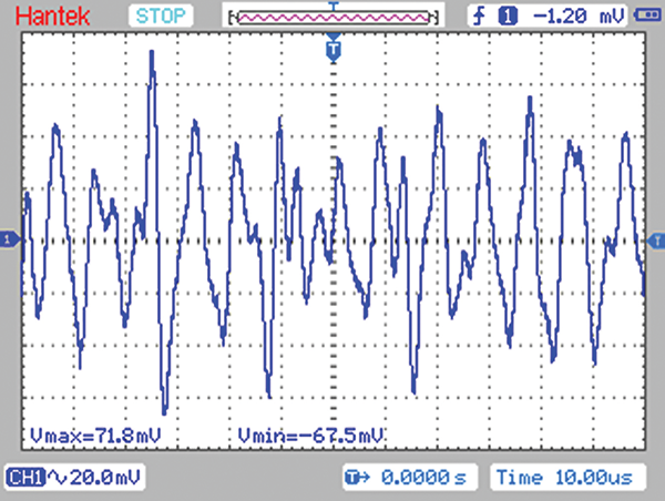
A digital oscilloscope has finite resolution – both its A/D converter and its screen, with typical resolution of 8-bit, or 256 steps. When the measured signal is in the lowest few bits, the oscilloscope adds to it its own noise and A/D dither, inflating the signal value. Unless the vertical scale is pegged up to maximum sensitivity already, the data in Figure 8a offers little value. In the ideal case the signal should occupy ~2/3 of the screen as shown in Figure 8b. The signal, the very same signal as in Figure 8a, but is now clearly visible and with more believable values. Watch for overload – if the signal is clipped on the screen, the front stage of the oscilloscope may be distorting the waveform and the measurements are no longer accurate.
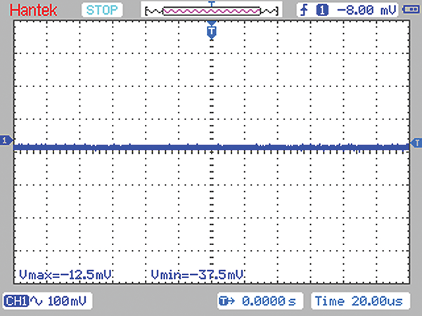
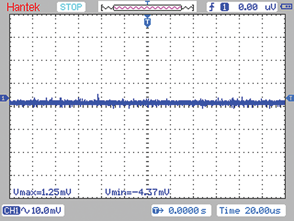
Figure 9 further illustrates importance of selecting the correct scale. In this case the signal is very low and is, essentially, flatlining. If one is to estimate the amplitude of the signal, Figure 9a would show an order of magnitude higher “noise level” than the much more realistic Figure 9b.
Time Base
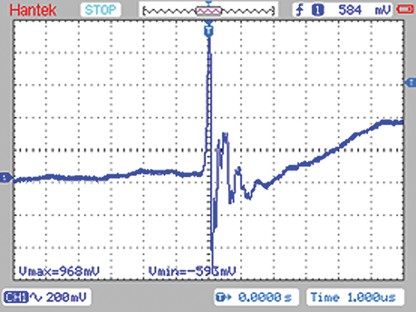
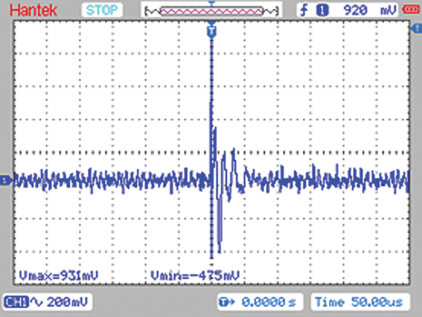
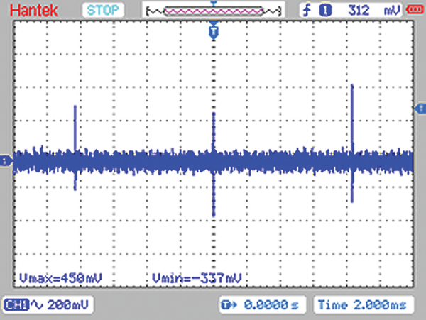
No less important than the vertical scale is the time scale. The same signal is shown in Figure 10. For a full evaluation of the signal any one of the screenshots of the same signal is insufficient. One needs all three screenshots to have a complete picture. One can see the rise time of the pulse in Figure 10a; the ringing of the signal in Figure 10b, and the repetition rate of the signal in Figure 10c (which in this case corresponds with the frequency of AC mains). The attentive reader would notice that the wider the time base, the lower the displayed amplitude of the signal. The oscilloscope resolution provides limitations not only on vertical scale but on horizontal (time) scale as well. The more we compress the signal on the screen, the fewer bits would represent the signal and the signal peak can be missed, lowering its perceived amplitude.
Triggering of an Oscilloscope
Triggering is perhaps the most important function in capturing the right signal. Figure 11 provides an illustration of that. A typical EMI signal consists of “important” parts such as A and B, “secondary” part C, and rather unimportant part D. If your trigger is set to “auto” you would see mostly signals D, occasionally C. The best trigger mode to use for EMI signals is “normal.” Initially, set the trigger level low and gradually raise it until the triggering stops and the waveform on the screen freezes.
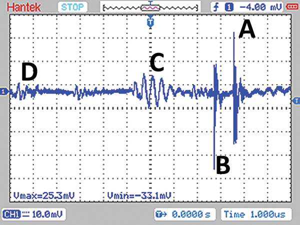
Note that signals A and B have similar maximum amplitude but different polarity. These peaks can be both positive and negative, therefore it is important to repeat capture with different trigger polarity.
We Have Done the Measurements – Now What?
The data by itself is of little consequence unless it is actionable. First, we need to know what the acceptable levels of EMI are and whether we need to do anything about our findings.
To the author’s knowledge, there is no IEC-level standard addressing broad industry needs for low levels of EMI. There are, however, some industry-specific documents specifying acceptable levels of EMI.
SEMI E176-1017 Guide to Assessing and Minimizing Electromagnetic Interference in a Semiconductor Manufacturing Environment
SEMI12 is an international consortium of semiconductor manufacturing and related companies working on improvements of productivity and advancing technology. Among other activities, SEMI sets standards for the industry covering many aspects of semiconductor manufacturing. The author is a co-chair of Metrics Committee of SEMI Standards overseeing, among other task forces, EMC Task Force, where he serves as a Task Force Leader. SEMI E176 Standard13 was well covered in this publication.14 Depending on the internal geometry of the semiconductor devices in the process allowable levels of EMI vary – the smaller the geometry the lower the allowable EMI levels. The same limits apply to adjacent industries – PCB assembly is not much different from semiconductor device manufacturing when it comes to device handling. Table 1 shows selected recommended EMI levels for different geometries of the devices.
| Category | Geometry | Radiated Near Field | Radiated Far Field | Conducted Emission | Ground Current |
| 1 | ≥28.3 nm | 2 V/m | 1 V/m | 0.3 V | 50 mA |
| 2 | 14.2 – 28.3 nm | 1.5 V/m | 0.8 V/m | 0.2 V | 20 mA |
| 3 | 10 – 14.2 nm | 1 V/m | 0.7 V/m | 0.1 V | 10 mA |
| 4 | 7.7 – 10 nm | 0.7 V/m | 0.5 V/m | 0.1 V | 5 mA |
Table 1: SEMI E176-1017 recommended emission levels in semiconductor manufacturing (partial data)
According to this table, the voltage between the robotic arm and the chassis shown in Figure 9 (400mV) exceeds even the most generous level of conducted emission – 0.3V. If you are reading this article, most likely your devices have smaller geometry, and are consequently more sensitive, and demanding lower levels of EMI.
IPC-A-610 Acceptability of Electronic Assemblies
IPC, an organization6 that governs the quality of electronic assemblies worldwide, publishes limits on electrical overstress in its Standard IPC-A-6106: “extremely sensitive components require that soldering irons, solder extractors, test instruments and other equipment must never generate spikes greater than 0.3 volt.” Note the emphasis on “spikes” in recognition that even a short transient can irreversibly damage a device. SEMI E176 Standard is also applicable for PCBA since there is very little difference, from an EMI point of view, in handling devices in an IC handler and in SMT pick-and-place machine
ANSI/ESD STM13.1 Electrical Soldering/Desoldering Hand Tools
This Standard Test Method (STM)15 created by EOS/ESD Association defines limits for AC and DC voltages on the tip of the iron itself, not in any application. The document is used to qualify soldering irons, not the soldering process including workbench. The only practical value we can use from this document is maximum allowed current of 10 mA.
Conclusion
Without proper measurements it is impossible to establish satisfactory EMI control. This article merely touches some key points of EMI measurements. The author hopes that this article demystifies EMI often considered a “black art” and makes it possible to use by anyone familiar with an oscilloscope.
Even if you are not overly concerned with EMI today, tomorrow you may be – sensitivity of components and of electronic circuits to EMI is continually increasing. You may be at a place where resolving EMI issues presents an urgent need rather than academic curiosity. The next step is mitigation of EMI in your process, but this is outside of the scope of this article.
References
- V. Kraz, “Electromagnetic Compliance – a View from the Field,” In Compliance Magazine, October 2017.
- TR23.0-01-20. ESD Association Technical Report for the Protection of EOS/ESD Susceptible Items – Electrical Overstress in Manufacturing and Test, EOS/ESD Association 2020.
- J. Salisbury, et. al. Reducing EOS Current in Hot Bar Process in Manufacturing of Fiberoptics Components, EOS/ESD Symposium, 2016.
- Bogdan Adamczyk, “Conducted Emissions Measurements: Voltage Method,” In Compliance Magazine, August 2017.
- K. Armstong, “Guide to Testing Conducted Emissions (Based on the Methods in EN 55022 and EN 55011),” In Compliance Magazine, July 2011.
- IPC-A-610G: Acceptability of Electronic Assemblies, http://www.ipc.org
- OnFILTER, Power Line EMI Adapters, https://www.onfilter.com/emi-measurements.
- R. Dorf, The Engineering Handbook, CRC Press, 2018.
- App. Note: CleanSweep® AC EMI Filters and UPS, OnFILTER.
- V. Kraz, S. Meyer, R. Fitzpatrick, “The Implementation of SEMI E176,” In Compliance Magazine, September 2019.
- T. Iben, et.al., EMI-Generated EOS in Wire Bonder, EOS/ESD Symposium, 2017.
- SEMI, http://www.semi.org.
- SEMI E176-1017 Guide to Assessing and Minimizing Electromagnetic Interference in a Semiconductor Manufacturing Environment.
- V. Kraz, “Dealing with EMI in Semiconductor Manufacturing: Part II,” In Compliance Magazine, May 2018.
- SI/ESD STM13.1 Electrical Soldering/Desoldering Hand Tools.
