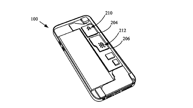
The patent application describes how an ultra-thin water resistant coating is applied to the printed circuit board (PCB) via a process called plasma-assisted chemical vapor deposition (PACVD). The surface of a substrate would be charged, and then the device would be placed in a vacuum chamber filled with fluoropolymer gas. When a voltage is applied to the gas, it turns into plasma and bonds to the substrate.
Of course the EMI shielding could block critical components. To mitigate this, Apple perforating the EMI shield above specific electrical components on the PCB. The holes would be large enough to let plasma in, but small enough to restrict the passage of EMI. Alternatively, in cases that require larger openings in the EMI shield, the perimeter of the opening would be masked with metal tape during the PACVD process. In regards to moisture potentially infiltrating board-to-board connectors, Apple’s document suggests that silicone seals would be applied.
Learn about the specific details by reading the full patent application.